Friday, October 31, 2014

Universal Battery Charger Battery charger for general purpose usage Universal Battery Charger circuit diagram The chargers output voltage is adjust

Universal Battery Charger

Battery charger for general purpose usage.

Universal
The chargers output voltage is adjustable and regulated, and has an adjustable constant-current charging circuit that makes it easy to use with most NiCad batteries. The charger can charge a single cell or a number of series-connected cells up to a maximum of 18V.

Power transistors Q1 and Q2 are connected as series regulators to control the battery chargers output voltage and charge-current rate. An LM-317 adjustable voltage regulator supplies the drive signal to the bases of power transistor Q1 and Q2. Potensiometer R9 sets the output-voltage level. A current sampling resistor, R8 (a 0.1 ohm/5W unit), is connected between the negative output lead and circuit ground. For each amp of charging current that flows through R8, a 100mV output is developed across it. The voltage developed across R8 is fed to one input of comparator U3. The other input of the comparator is connected to variable resistor R10.

As the charging voltage across the battery begins to drop, the current through R8 decrease. Then the voltage feeding pin 5 of U3 decreases, and the comparator output follows, turning Q3 back off, which completes the signals circular path to regulate the batterys charging current.

The charging current can be set by adjusting R10 for the desired current. The circuits output voltage is set by R9
Read More..

Crowbar Speaker Protection Circuit Diagram

Crowbar circuits are so-called because their operation is the equivalent of dropping a crowbar (large steel digging implement) across the terminals. It is only ever used as a last resort, and can only be used where the attached circuit is properly fused or incorporates other protective measures.

A crowbar circuit is potentially destructive - if the circuitry only has a minor fault, it will be a major fault by the time a crowbar has done its job. It is not uncommon for the crowbar circuit to be destroyed as well - the purpose is to protect the device(s) attached to the circuit - in this case, a loudspeaker.

Description

Theres really nothing to it. A resistor / capacitor circuit isolates the trigger circuit from normal AC signals. Should there be enough DC to activate the DIAC trigger, the cap is discharged into the gate of the TRIAC, which instantly turns on ... hard. A TRIAC has two basic states, on and off. The in-between state exists, but is so fast that it can be ignored for all intents and purposes.

Crowbar Figure 1 - Crowbar Speaker Protector

The BR100 DIAC (or the equivalent DB3 from ST Microelectronics) is rated for a breakdown voltage of between 28 and 36V - these are not precision devices. Needless to say, using the circuit with supply voltages less than around 40V is not recommended, as you will have a false sense of security. The supply voltage must be higher than the breakdown voltage of the DIAC, or it cannot conduct. Zeners cannot be used as a substitute for lower voltages - a DIAC has a negative impedance characteristic, so when it conducts, it will dump almost the full charge in C1 into the gate of the TRIAC. This is essential to make sure the TRIAC is switched into conduction.

The TRIAC is a common type, and may be substituted if you know the specifications. Its rated at 12A, but the peak current (non-repetitive) is 95A, and it only needs to sustain that until the fuse (or an output transistor) blows. A heatsink is preferred, but there is a good chance that the TRIAC will blow up if it has to protect your speakers, so it may not matter too much. The 0.47 ohm resistor is simply to ensure that the short circuit isnt absolute. This will limit the current a little, and increases the chance that the TRIAC will survive (albeit marginally). Feel free to use a BT139 if it makes you feel better - these are rated at 16A continuous, and 140A non-repetitive peak current.

The peak short circuit current will typically be about 90A for a ±60V supply, allowing ~0.2 ohms for wiring resistance and the intrinsic internal resistance of the TRIAC, plus the equivalent series resistance of the filter capacitors. Thats a seriously high current, and it will do an injury to anything thats part of the discharge path. Such high currents are not advised for filter caps either, but being non-repetitive they will almost certainly survive.

Construction & Use

Apart from the obvious requirement that you dont make any mistakes, construction is not critical. Wiring needs to be of a reasonable gauge, and should be tied down with cable ties or similar. C1 must be polyester. While a non-polarised electrolytic would seem to be acceptable, the circuit will operate if the capacitor should dry out over the years. This means it will lose capacitance, and at some point, the crowbar may operate on normal programme material. This would not be good, as it will blow up your amplifier!

Make sure that all connections are secure and well soldered. Remember that this is the last chance for your speakers, so it needs to be able to remain inactive for years and years - hopefully it will never happen. The circuit doesnt have to be mounted in the amplifier chassis - it can be installed in your speaker cabinet. Nothing gets hot unless it operates, at which point no-one really cares - it just has to save the speakers from destruction once to have been worthwhile.

Remember that the crowbar circuit absolutely must never be allowed to operate with any normal signal. A perfectly good amplifier that triggers the circuit because of a high-level bass signal (for example) will very likely be seriously damaged if the crowbar activates. To verify that no signal can trigger it, you may want to (temporarily) use a small lamp in place of R2, and drive the amp to maximum power with bass-heavy material.

A speaker does not need to be connected. If the lamp flashes, your amp would have been damaged. If this occurs, you may want to increase the value of C1. Note that bipolar electrolytics should never be used for C1, because they can dry out and lose capacitance as they age. This could cause the circuit to false-trigger.
Read More..

Inverter Circuit for Soldering Iron

The following inverter circuit can be used to supply soldering iron or other small electronic devices which need up to about 50W / 230V power supply.

Inverter


Transistors T1 and T2 (each BC547) form an astable multivibrator that creates 50Hz signal. The complementary outputs from the collectors of transistors T1 and T2 are fed to pnp Darlington driver stages formed by transistor pairs T3-T5 and T4-T6 (utilising BC558 and BD140). The outputs from the drivers are fed to transistors T7 and T8 (each and every 2N3055) connected for push-pull operation. Use suitable heat-sinks for transistors T5 via T8.

A 230V AC primary to 12V-0-12V, 4.5A secondary transformer (X1) is utilised. The centre-tapped terminal of the secondary of the transformer is connected to the battery (12V, 7Ah), whilst the other two terminals of the secondary are connected to the collectors of power transistors T7 and T8, respectively.

Whenever you power the circuit making use of switch S1, transformer X1 produces 230V AC at its primary terminal. This voltage could be employed to heat your soldering iron.

Build the circuit on a standard purpose PCB and place it in a suitable cabinet. Hook up the battery and transformer with proper current-carrying wires. On the front panel of the box, fit power switch S1 along with a 3-pin socket for connecting the soldering iron.

Note that the ratings of the battery, transistors T7 and T8, and transformer could vary as these all depend on the load (soldering iron).
Read More..

Thursday, October 30, 2014

Wire Loop Game Circuit Diagram

In the ‘Wire Loop Game’, a test of dexterity,  the player has to pass a metal hoop along a  twisted piece of wire without letting the hoop  touch the wire. Usually all the associated electronics does is ring a bell to indicate when the  player has lost. The version described here has  a few extra features to make things a bit more  exciting, adding a time limit to the game and a ticking sound during play. 

Two 555 timer ICs are used to provide these  functions. IC1 is configured as a monostable which controls the time allowed for the  game, adjustable using potentiometer P1. IC2  is a multivibrator to provide the ticking and Two 555 timer ICs are used to provide these  functions. IC1 is configured as a monostable which controls the time allowed for the  game, adjustable using potentiometer P1. IC2  is a multivibrator to provide the ticking and he continuous buzz that indicates when the  player has touched the wire with the hoop. 

Wire Loop Game Circuit diagram :


Wire Loop Game Circuit Diagram

When the monostable is in its steady state,  the output of IC1 (pin 3) is low. T1 acts as  an inverter, and D2 is thus forward biased.  R8 and R4 are therefore effectively in parallel, with the result that IC2 produces a low audible tone. The value of R4 is considerably  greater than that of R8, and so the frequency  of the buzz generated by IC2 is chiefly deter-mined by the value of R8.

When the monostable is triggered, the high  level at the output of IC1 is again inverted  by T1. D2 is reverse biased and so R8 is effectively removed from the circuit. The frequency of IC2 is now largely determined by  the value of R4. The ratio of R4 to R5 and the  value of C4 affect the mark and space periods for the multivibrator: for a satisfactory  ticking sound short pulses with long gaps  between work well. 

Whether a sound is produced also depends  on the voltage on pin 4 of IC2. When the 9 V  supply is connected the monostable is initially inactive and there is no voltage across  C1. Pin 4 (reset) on IC2 is thus low and no tone  is produced. IC1 is activated by a brief press of  S1, which generates a low-going trigger signal  on pin 2 to start the game. C1 now charges via  D1 and IC2 is allowed to oscillate, generating  the ticking sound. 

The pulse width of the monostable sets the  game duration, and can be adjusted using  P1. If the allowed time expires, or if the reset  input to IC1 is taken low (which happens when the hoop touches the wire), the monostable  returns to the quiescent state. This causes IC2  to generate the low buzz sound. D1 is now  reverse biased and C1 discharges through the  relatively high-valued resistor R9. After a few  seconds the voltage across C1 falls sufficiently  that the buzz stops and the circuit is ready for  the next player. 

The circuit can be built first on a breadboard,  so that the component values can easily be changed to suit particular preferences for  game duration and buzz pitch. When suitable  values have been selected the circuit can be  built more permanently on a printed circuit  board. The author used a sheet of plywood  to form a base for the game, the twisted wire  being fixed to the board and wired to the electronics mounted below it. 


Author: Andreas Binner
Read More..

Subwoofers are the quality car sound

Car subwoofers are the life of a quality car sound organization. Basically, subwoofers are nothing supplementary than bonus speakers attached to your sound system. Car subwoofers might be situated passive otherwise powered. Passive woofers obtain their power from the cars audio arrangement, but a powered subwoofer derives its power independently. These days, indoors keeping with the newest technologies, car subwoofers draw closer in all shapes, sizes and flag. 

being you could know, altered speakers attached to amplifiers hand over different frequencies of sounds. Subwoofers attached to an amplifier deliver low frequency low sounds in the song. In usual sound systems, the octaves are missing. in the main, listeners puzzle out not yearn for these sounds either. But if you fancy the rich and varied sounds of harmony, before if you covet to listen in to deep tracks (composition with the aim of has been personally formed instead of low), you would miss subwoofers willfully. Car subwoofers are a should if you want the car to echo with the beat of your melody. 

round about of the paramount car subwoofers include Sony, Alpine and Kenwood. both of these products is well priced and delivers sharp quality sound. However, carry out run a voice check or you try ready slightly of these subwoofers since except the subwoofer delivers deep sounds, you might when well try with no them. You in addition need a subwoofer procedure with the purpose of good wishes the be and day of your vehicle.

Car subwoofers might range from 8 inches to 60 inches. nearly everyone subs are mounted clothed in boxes. But these days you can and urge them in a tube mounted format. usually, the subwoofer choice give rise to the amplifier connected to it so in the same way as to help it give the vital sound. Since power supplies are quite above what is usual in subwoofers and since you need accurate power supply to deliver high quality sounds, an amplifier is pretty much a obligation on behalf of subwoofers. 

While business your car subwoofer, the key phenomenon you have to decide is everyplace to obtain it from. A integer of selections are open online, and a allocation of them are competitively priced. But, make it a aim to buy from apparent online dealers. after that, decide on the funds. Subwoofers are a luxury; they greet rations with the purpose of are ended and exceeding common expectations. So, solve not try to scrimp and save. lead to on behalf of the paramount quality subwoofers your financial statement desire allow. Longevity and quality matters. If you cannot afford regular prices, try not on online auctions. You can bag selected real bargains on time. then again, you could in addition consider exchange quality subwoofers with the aim of be inflicted with been used, but are inwards sound condition. A miniature caution and sensible selection spirit assent to you have a sound arrangement with the intention of is next to nothing. 

Ask a few car audiophile, and they will acquaint with you that you simply cannot make with a car subwoofer. a long time ago you catch hooked to the pleasure of listening to right, extraordinary quality sound, you would remain singing the same pitch (excuse the pun).

7 Elephants has been a main distributor of many brands of car audio equipment such in the role of Pioneer, Kenwood, JVC, Sony, Panasonic and extra on reasonable prices.
Read More..

Railway Points Sequencer Circuit Diagram

Dedicated model rail enthusiasts using sophisticated train and points controllers often have the problem that as their layouts get bigger and more complex, the transformer supplying power to the points does not have enough current to switch several points at the same time. The actuators in the points are designed for ac operation so it doesn’t help by rectifying the supply and adding reservoir capacitors, the coils can overheat and burn out if they get jammed during their travel (ac operation actually helps to overcome friction in the mechanism). The circuit shown here solves this problem by using a sequencer to ensure than only one points actuator can be active at any point in time. During operation the controller will switch all the points on one line at the same time as usual, but the other connection to each coil is connected to the sequencer unit. This circuit will only allow current to flow through one coil at a time. 

Railway Points Sequencer Circuit diagram :
Railway Railway Points Sequencer Circuit Diagram

The sequencer circuit consists of a 555 timer configured as an astable multivibrator clocking a 4017 Johnson counter where the ten outputs are used to switch ten triacs in sequence, enough for ten sets of points. P1 alters the oscillator frequency of the 555 timer and can be adjusted so that each time interval of the sequencer is long enough to allow the points to switch. 

The switching time varies depending on the type of points but is typically between 1 s and 1.5 s. Any points that jam during switching give out a characteristic humming noise in time to the switching frequency so it makes them easier to find. The eleventh output of the 4017 can be connected to an LED (together with a series resistor). This will flash to give a visual indication of the sequencers operation. Power for the circuit is provided by 15 V ac from the points transformer. The B80C1500 bridge rectifier (80 Vpiv, 1.5 A) and regulator IC1 produce a stabilised 12 V for the circuit. Current consumption is only a few milliamps.
Read More..

Dice digital circuits

A electronic associates was seeking a compete circuits happening your boundless stage,a low-priced and comfortable to made. This dice digital circuit would be present a favorite of everybody, by using it to present the statistics.

Dice

As soon as you switch to a spin button or else it like is tossing a dice. Looks like a random form normally. A sympathy of this circuit,an a gang oscillator 1Khz with IC 555 and RC networks,it bidding be real output to IC2 is Decade counter IC - 4017. As soon as I aim inedible the spin switch, it will be converted to a binary input with a diode matrix D1-D9 (1N4148 before come to 1N914) and therefore misrepresented to a 7 segment exhibit with a decoder drive IC rejection. CD4511 (IC3). The brightness of the numeric display, may well transpire customized by adjusting the help of R3.
Read More..

Wednesday, October 29, 2014

TDA2050 Power Amplifier Circuit

High output power, low distortion, power amp for HiFi and high class TV sets. Maximum output at 4 ohm speaker is 35 watts, while the 8 ohm speaker is only 15 watts. This circuit must use a good power supply so that the sound quality could be as expected.

TDA2050

List of components:
     Resistors 1, 2, 3, 4: 22K ohm
     5 resistor: 2.2 ohm
     Capacitor 1: 100uF/50V
     Capacitor 2: 2.2uf/50V
     Capacitor 3: 22uF/50V
     Capacitor 4: 0.47uF
     Capacitor 5: 1000uF/50V
     Capacitor 6: 100nF
     Capacitor 7: 1000uF/50V
     IC: TDA2050
Read More..

TA8259H bassed 4 channel car amplifier Diagram Circuit


Using the TA8259H integrated circuit can be designed a very simple 4 ch BTL audio power amplifier for car audio application.
This IC can generate more high power: POUT MAX = 37 W as it is included the pure complementary PNP and NPN transistor output stage.

It is designed low distortion ratio for 4 ch BTL audio power amplifier, built-in Stand-by Function, Muting Function, Clip detector, and diagnosis circuit.
As you can see in the circuit diagram , this audio amplifier electronic project require extreme low external electronic parts .

Additionally, the AUX. amplifier is built-in, it can make the beep signal etc. output to 2 channels (OUT1 and 4).

Input voltage range that is accepted by this audio amplifier project is between 9 and 18 volt , but typically is required a 14,4 volts DC.
All speakers used with this amplifier circuit project , based on TA8259H IC must have a 4 ohms impedance .
Read More..

LG Gx2 5 7 inch cell with the same laser technology in LG Camera G3

LG
LG is presenting streak new cell before IFA 2014 Earlier this week the company introduced the LG Stylus G3 to challenge the Samsung Galaxy Note, but apparently thats not all you have prepared and presented the LG Gx2, which can be easily confused with the LG G2x years ago.

The new LG cell Gx2 also wants to enter the territory of the Samsung Galaxy Note to have a 5.7 ​​inch screen, but its specifications are still being average and not high end.

Gx2 LG screen has a resolution HD (720p), a quad-core 1.2GHz processor, 1.5GB of RAM and 8GB of storage.

Additionally, the cell has a ATTERY of 3,200mAh, a rear 8 megapixel camera, 1.3 megapixel front camera and battery 3,200mAh. The rear camera has the same technology found in the LG G3, mainly the laser autofocus.

LG has not announced when it would be released in that country and what would be its price. However, there is the possibility that, for the moment, leave only in Asia, but do not rule out the possibility of reaching other markets in the future.
Read More..

Tiny Door Guard Alarm Circuit Diagram

If some intruder tries to open the door of your house, this circuit sounds an alarm to alert you against the attempted intrusion. The circuit (Fig. 1) uses readily available, low-cost components. For compactness, an alkaline 12V battery is used for powering the unit. Input DC supply is further regulated to a steady DC voltage of 5V by 3-pin regulator IC 7805 (IC2).


Tiny
Fig. 1: Circuit of the door guard

Assemble the unit on a general-purpose PCB as shown in Fig. 4 and mount the same on the door as shown in Fig. 3. Now mount a piece of mirror on the door frame such that it is exactly aligned with the unit. Pin configurations of IC UM3561 and transistors 2N5777 and BC547 are shown in Fig. 2. 

UM3561
Fig. 2: Pin configurations of UM3561 and transistors 2N5777 and BC547

Initially, when the door is closed, the infrared (IR) beam transmitted by IR LED1 is reflected (by the mirror) back to phototransistor 2N5777 (T1). The IR beam falling on phototransistor T1 reverse biases npn transistor T2 and IC1 does not get positive supply at its pin 5. As a result, no tone is produced at its output pin 3 and the loudspeaker remains silent. Resistor R1 limits the operating current for the IR LED.
When the door isopened, the absence of IR rays at phototransistor T1 forward biases npn transistor T2, which provides supply to  positiveIC1. Now 3-sirensound generator IC UM3561 (IC1) gets power via resistor R5. The output of IC1 at pin 3 is amplified by Darlington-pair transistors T3 and T4 to produce the alert tone via the loudspeaker. 

Back
Fig. 3: Back view of the door assembly

Rotary switch S2 is used to select the three preprogrammed tones of IC1. IC1 produces fire engine, police and ambulance siren sounds when its pin 6 is connected to point F, P or A, respectively.

Suggested
Fig. 4: Suggested enclosure with major components layout


Author : T.K. Hareendran - Copyright : EFY
Read More..

Tuesday, October 28, 2014

VHF UHF Low Noise amplifiers MAX2664 MAX2665 circuit

A very simple low cost and ultra compact VHF UHF Low-Noise amplifiers circuit can be designed using the MAX2664 and MAX2665 ultra-compact LNAs for VHF/UHF applications.
These devices incorporate a broadband LNA with an integrated bypass switch. The MAX2664 covers the UHF frequency range from 470MHz to 860MHz, and the MAX2665 covers the VHF frequency range from 75MHz to 230MHz. Each device has a zero-power bypass mode for improved high-signal-level handling conditions.
 As you can see in the presented circuit diagram , this RF project requires very few external components . Both ICs has a high gain around 15dB and require a single power supply , that can provide an output voltage between 2.4 to 3.5 volts .
VHF UHF Low-Noise amplifiers has a very low current consumption of 3.3 mA and can be used in applications like : Smartphones/Handsets , MP3 Players , Home Audio/Video and other portable navigation devices .
Read More..

Mosfet High Power Amplifier complete PCB

Amplifier
Amplifier circuit is finished, and ready for use.
1000W High Power Amplifier MOSFET LEGEND stage Master MK2 is a very high-quality and powerful amplifier. It is not into the classroom HiEnd for sure, but very respectable sounding element with lots of of power. It was not designed with national interior because the primary goal already, such a power used barely rarely at home the board and interior with the exception of perhaps in a few superior nightclubs. Frankly, due to a tall performance, may possibly helper light to a certain extent proceed categorize, but other specifications and significant quality on the supporter values and needs! My no more than other submission meant for you to think approaching it on extent, Master internship in the role of a Master MK2. Internship Master 500…1000W, but is a a tiny easier (and cheaper) to build. ” PCB present in this fashion as beneath 1000W Mosfet PCB 1000W mosfet PCB.

1000W
1000W High Power Amplifier with Mosfet Circuit Schematic Diagram
Printed
PCB design for this Amplifier Circuit
Read More..

Minimal low supply rail detection

At this point’s a minimal low supply rail detection circuit with the purpose of expenditure peanuts and takes a short time ago 20 minutes or else so to become. Its power consumption is quite low, so it may perhaps definitely survive built into battery-powered campaign. as an alternative of using an op amp, the circuit is built around three low-cost transistors (Q1-Q3). Diodes D1-D3 form a 1.8V voltage reference (Vref) used for the emitter of Q1. If the voltage across the voltage wall formed by R1 and VR1 is a reduced amount of than this, Q1 turns on and food Q2 with foundation bias current.

Rail

This turns on Q3 here proportion to this bias current which subsequently drives LED1. The brightness of the LED gives an indication of the severity of the low voltage condition. The brighter the LED, the minor the supply voltage. Trimpot VR1 is adjusted so to facilitate LED1 really comes on by the desired low-voltage promontory. The current consumption is typically take away than 2mA at what time LED1 is rotten. in conclusion, the price exposed in support of RLED is right for 6-12V surgery. For other voltages, RLED can ensue calculated using the formula RLED = (Vcc - 1.8)/0.01 (this equates to a current of with reference to 10mA).
Read More..

Simple 150 Watt Power Amplifier Circuit

This is the very simple circuit diagram of 150W power amplifier. The circuit is easy enough to built without PCB. The power output range is about 100-150W depends to the power supply and the Darlington’s you use for the amplifier. Heatsink is a must since the final transistor is going to hot when the amplifier is activated.

Simple


The amplifier requires split power supply. The transformer is depending to your home electrical installation, it can be 110V or 220V primary. Use 35V-0-35V secondary (transformer output), you will get about 45V DC output from transformer 35V AC after rectified by the diodes. The Transformer current output should be at least 4A for better audio performance. Use 4A / 100V diodes.
Read More..

Monday, October 27, 2014

Power Amplifier Protector

Now you can protect your HiFi amplifier from damage due to overheating. This circuit will cut off power to the amplifier board at the time the temperature was high. Automatically connect the power when the temperature returns to normal. This circuit uses a sensor NTC Thermister heat and also has a warning sound and reset determination.

Amplifier circuit protector is using popular timer IC NE 555 as the temperature controlled switch. The trigger pin 2 is connected to a potential divider consisting Thermister VR and NTC. Thus the voltage on pin 2 depending on the resilience and determination Thermister VR. NTC (Negative Temperature Coefficient) Thermister has a high resistance in the normal temperature and the resistance decreases as temperature increases. Threshold pin 6 of IC is used to reset the IC if necessary. When the pin 6 voltage gets higher than the IC pin 2 will reset and the output is low.

Power Amplifier Protector  Circuits

Power to the amplifier board is given by (NC) contact is usually connected from the relay and the switch S2. So that power to the amplifier board will be available through the NC contacts of the relay when the relay S2 and the state is not powered. Thermister resistance is governed by VR triggering pin 2 of IC peaks at normal temperatures. When the temperature inside the cabinet amplifier increases, resistance decreases so that it becomes conductive Thermister. This makes the trigger pin 2 of IC is low and its output is high. T1 works so that the relay energizes and the ringing of a bell. This will damage the electrical supply to the amplifier board. Relay will not be automatically powered when the temperature returns to normal.

Amplifier circuit protectors are very useful to protect your home sound system.
Read More..

NCS8353 20 W stereo Class D audio amplifier Diagram Circuit


A very simple stereo Class D audio amplifier electronic circuit project can be designed using the NCS8353 audio IC capable of delivering a continuous power of up to 20 W/ch into an 8 ohms .
NCS8353 stereo Class D audio amplifier circuit is designed by ON Semiconductor and it can be powered from the existing 24 V rail in Flat Panel Television (FPTV) systems. The high efficiency of the NCS8353, 86%, reduces the requirement of an external heat sink when driving high power.

The digital power limit feature can program the output power limit at 10 W, 12 W, 15 W, or 20 W/ch, allowing the NCS8353 to be a single system solution in FPTV audio applications.
The digital power limiter quickly reduces the internal gain of the amplifier when high amplitude signals would cause excessive clipping on the output.
The gain of the NCS8353 is programmed via two gain pins, G0 and G1, allowing four selectable ranges: 20 dB, 26 dB, 32 dB, and 36 dB.
Auto recovery short circuit and over temperature protection circuitry are incorporated to ensure device functionality after short circuit and high temperature events occur .
The circuit can be powered from a wide input voltage range from 8 volt DC up to 26 volt DC .

Read More..

Lead Acid Battery Charger LM317

Lead Acid Battery Charger circuit is highly recommended to recharge battery. And recommended that maximum voltage 24V 7A battery, so you can recharge a battery simultaneously. Battery Charger has been little use of several components such as diodes, electrolytic capacitors, transistors, resistors, and also for strengthening of the voltage and current stresses. And also do not forget to lowering electric voltage 220V to 20V-35V 5-10 Ampere suitable for Lead Acid Battery Charger circuit.
for Figure Schematic circuit Lead Acid Battery Charger, you can see below :


List of components for the circuit Lead Acid battery:

R1               = 1Ω 2w
R2               = 100Ω
R3               = 220Ω
R4               = 10KΩ Trim
D1 - D5       = IN4004
Q1               = BC547
IC 1             = LM317
C1 - C2       = 1000µF 50V
C3               = 470µF 50V

Transformer I mentioned above can use the 5A - 10A with a secondary voltage of about 20Volt-35Volt AC. My advice to IC please be cooler, because when the circuit and well even IC LM317 works it causes IC hot. Also to assemble the components using PCB (Printed works Circuit Board) qualified with a good track, as well as the components that will be used not forget to check back whether good or not, so it will also produce good results.
Read More..

How Regulator with 2 Photocoupler

Working of Regulator with 2 Photocoupler that is :
  • Photocoupler N901 - used as a coupling-off control on the regulator by mikrokontrol. Which is set high and low voltage B + (st-by at the B + voltage is low). Control of the pin-37 POWER mikrokontrol → V610 → VD913 V908 → N901.
  • Photocoupler N903 - used to control on-off the regulator of X-ray circuit protector. X-ray protector circuit of flyback → VD451 → VD452 → SCR VS472. If the flyback voltage regulator over the job will automatically be turned off by N903
  • To disable the X-ray circuit protector, it can be temporarily removed photocoupler N903 first. In normal conditions the voltage at the transistor V474 should be zero.

Regulator Schematics
Trobelshuting there is no voltage for 5v st-by on the secondary :

  1. Disable by removing the first circuit protectors N903
  2. Check the voltage of 300V
  3. Check all transistors
  4. Check the start voltage of 300V by R909 >> R906 to the base of transistor power regulator
  5. Check the feedback C910 >> R904 (to oscillate)
Read More..

Sunday, October 26, 2014

5000W High Power Amplifier Audio Circuits

The High Power Amplifier has great advantages are 5000W ultra-light, high-power audio amplifier, without switching-mode power supply. This ambit is of an 2 x 2,500W RMS Stereo amplifier, super-light and after switching-mode ability supply. The ambit aloof shows a channel, and the ability accumulation that it assists to the two channels. The audio ambit should be duplicated, but the ability accumulation assists to the two channels after problems.

Click To view larger | 5000W High Power Amplifier Audio Circuits Diagrams

A adapted affliction should be destined to the careful agent of the audio line, that should be of audio-high-quality, of the blazon acclimated in microphone pre amps ascribe line. The accomplished accumulation (2 channels) of 5,000W RMS it should not counterbalance added than 32 lbs, already central of an adapted brownish box.

WARNING:
This ambit is alone for abecedarian use. It contains not-isolated genitalia of the electric AC net and it can be actual dangerous. The access for the speakers are not abandoned of the calm AC net and it requests added care. This action seeks to acting a accepted ability accumulation with abundant weight and amount reduction, after necessarily to use a switching-mode ability supply.

This action cannot be accustomed in some countries for commercial-use. The columnist doesn’t accept any albatross for the anatomy as that ambit it will be applied.
Read More..

LA4460 Simple Audio Amplifier

A unpretentious audio amplifier circuit can happen designed using the LA4460 IC . This circuit is very simple and require little exterior electronic components . The LA4460 IC is in fact used on behalf of car broadcasting or else car audio power amplifier and could provide output power up to 12 W. But at home this circuit is solitary used 5W.
LA4460 Audio Amplifier Circuit
This amplifier circuit can come about used for car means of communication applications , small screen , or else around other audio circuits so as to don’t require vast power .
explanation:
  1. work 12VDC to supply the circuit.
  2. Mount the LA4460 IC  with an appropriate high temperature sink
  3. Some of as a rule worthy skin of the LA4460 IC are : reverse connection protection , muting function,thermal runaway protection circuit ,completed voltage & pitch voltage protection circuit, load stunted-circuit current limiting protection circuit, output pins DC short-circuit protection.
Read More..

A Frequency Doubler Effect for Electric Guitar


This circuit is a octave shifting that is used for electric guitar is done by rectifying the original signal, just like AC to DC conversion inside your AC-DC power supply adapter. This circuit is use single supply instead of symmetric power supply. This is the figure of the circuit.
The rectifying is done by four 1N4148 silicon diodes, configured as full-wave rectifier bridges. Because the bridge is inserted inside the negative feedback of the operational amplifier (op-amp) U1B, the nonlinear characteristic of the diodes around the turn-on point (the forward bias voltage) is compensated by the op-amp’s feedback mechanism. 
Read More..

Saturday, October 25, 2014

LM741 Active high pass filter circuit


This is active high pass filter circuit for 327Hz frequency using LM741. It will use to build Harmonic at 3 of 130.81 frequency have the value at least. More than the frequency Fundamental 30 dB, for output be sawtooth wave form for use in sound of music way system Electronic design will use the circuit filters three rank frequency. By have 3 dB you slopes can use Op-amp IC number LM741 or number LF351it will meet the frequency well.
Read More..

Friday, October 24, 2014

Traffic Lights Circuit

The circuit of traffic lights in my opinion is a series of easy-hard-easy to make. 


Traffic

Where we are required to be able to condition the flame of three lamps by following the existing traffic regulations. If we use computer programming as a regulator of the third condition of the lights probably we will not spend too much time to make it. As an example with microcontroller programming or programming-based computer applications such as Visual Basic, Delphi and many others. But if you use a common electronic circuit components used may be somewhat time consuming to get the results you are fully in accordance with the conditions of traffic lights that use the streets.

Well ... if youre looking for examples of a series of simple traffic light above the range can I recommend to you. The working principle of a series of traffic light above is very easy to understand. The series of above use the output from IC up / down counter 74 190 as the producer output tercacah and then conditioned using logic gates so that the logic in accordance with the logic of the actual traffic light. Actually you can also use the IC counter ups as pencacahnya. Red lights are represented by the LED D1, D2 and yellow by green led by led D3.

LIST OF COMPONENTS:
Resistors: R1 (1 Kohm), R2, R3 and R4 (220 ohms) and VR1 (Potensio 10 K / 15 K)
Capacitors: C1 (100 UF)
Led: D1 (red), D2 (yellow) and D3 (green).
Integrated Circuit: IC1 (NE 555), IC2 (74LS190) and IC3 (74LS02)

HOW TO WORK AND ANALYSIS OF CIRCUIT LIGHT TRAFFIC:
To generate the signal used peggerak counter circuit astable circuit IC555.
R1, C1 and VR1 is a combination astable as a determinant of the speed of the clock signal to be inserted to the input counter and in the end will determine the length of time the flame of their lamps. The greater the value of the three clock cycles will stay longer and vice versa.
To obtain a combination of LEDs required only 2 bits output from the counter circuit.
Bit-3 from the output to the counter only be used as reset the enumeration.
The lamp was first lit the light yellow color, due to connect with the output Q1 of counter IC. Then followed by a red lamp that is connected to the output Q2. Then both (yellow and red) light simultaneously. The last green light will turn on its own.
The series of bit counter counts up with the sequence:
- 0 1 (light yellow light)
- 1 0 (red light)
- 1 1 (light yellow and red lights)
- 0 0 (light turned green, according to the nature of the gate NOR)
Examples of traffic light sequence apply only to one lane for traffic light circuit that uses more than one line then you can use the same circuit device and use a combination of gates as a liaison between the conditions of each lane. This means you should make a longer red light is illuminated on each other point for point which it operates. These conditions can be achieved by utilizing a combination of logic gates in a chain.
Read More..

LM4651 and LM4652 170W power amplifier

170 Watt power amplifier is a power amplifier that is built by IC LM4651 and LM4652.
Part of this power amplifier driver using the LM4651 IC designed specifically for the purpose of the class AB amplifier driver with short circuit protection feature, containing under voltage, thermal shutdown protection and standby functions. Section 170 Watt power amplifier using LM4651 IC with a MOSFET power amplifier is equipped with temperature sensors that will be used by IC LM4651 as controlnya thermal signal. IC IC LM4651 and LM4652 are designed specifically to each other in pairs to create a class AB power amplifier with protection features are detailed. Detailed series of 170 Watt power amplifier can be seen in thethe following figure .

LM4651

Power amplifier circuit requires supply voltages +22 V DC symmetrical 0-22V. Power Amplifier with IC LM4651 and LM4652 are often used in portable HiFi systems such as powered speakers, power subwoofer and car audio power Booter. D1, D2, D3 and D4 in series 170 watt power amplifier with LM4651 and LM4652 is a 22V zener diode.
Read More..

Thursday, October 23, 2014

Make a series letters from the LED

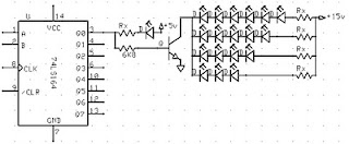
Make a series letters from the LED , Things to consider before making the sign of the LED array,
1) Use LED nodes.
2) Paint the top of the PCB with a dark color (black).
3) Note the LED specifications. In this experiment use a 5mm diameter LED nodes
that emit red, specification voltage of 3 volts.

The assembly of LED:
1) One letter composed at most 5 columns and 7 rows.
2) One column mostly composed by 6 LEDs are arranged series.
3) Then the fifth column are connected in parallel.
4) Each column given the constraints, Rx, which amount depends on the number of LEDs in one column and depends also on the type of LED (in this experiment that used LED 5mm in diameter, clear with red light beam).
5) In a column consisting of 6 LEDs, Rx = 330 ohm, 5 LEDs, Rx = 560 Ohms, 4 LEDs, Rx = 680 Ohms
Remember, this provision applies to 5 mm LED red light beam nodes.
6) Every letter was given FCS9013 transistor amplifier.

Here is one letter LED scheme.
Make


Medium picture below is the lay out of the 2-letter nameplate. To make the sign 8 letter, copied from a second stay this letter.

Make


Example of LED on the letters A and B:

Make

Value Rx in the first and the fifth column (letter A) of 560 ohms, because it consists of 5 LEDs are arranged series. Rx in the second column, third, and fourth, amounting to 680 ohms because it consists of two LEDs.
Rx first column letter B, 330 ohms. Rx second column, third, fourth, and fifth at 680 ohms.
Read More..

12V 3A Power Supply Circuit Diagram

This circuit provides a 12V regu-lated power supply with output current up to 3 amperes. It is spe-cially designed for use with 2m handheld rigs with linear power amplifier and CB portable QRP rigs. The circuit uses monolithic IC CA3085 voltage regulator in 8-lead TO-5 package.  Its salient features include good load and line regulation, output current up to 100 mA (which can be increased to several amperes with additional pass transistors), output short-circuit protection, and lower input voltage.  A low power dissipation is achieved by driving external series-pass transistor 2N4241 (T1) from  pin 2 of CA3085.
Circuit diagram :
12V, 3A Power Supply-Circuit-Diagram
12V, 3A Power Supply Circuit Diagram
Normal output pin 8 is returned to ground via diodes D3 and D4 to ensure error am-plification operation in the linear region. Ripple rejection is approximately 50 dB on no load and 35 dB on full load.  A 2x2x2.5cm aluminium heat sink fas-tened onto a 1.5mm blackened aluminium sheet of 12.5cm2 area on 2N4241 helps the circuit in dissipating heat without ex-ceeding maximum device ratings. CA3085 can dissipate up to 650mW power in free air, without any heat sink.  AFCO-make C-05-4 heat sink is suitable for this IC. An improper heat sink may cause device junction temperature to ex-ceed the limit, resulting in progressive deterioration of the device. 


Read More..

0 3 to 1 5V LED Flashlight

Circuit Project: 0.3 to 1.5V LED Flashlight

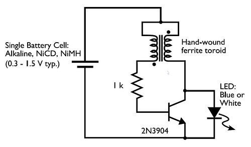
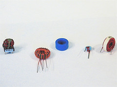
Its a little wisp of a circuit that allows you to drive a blue or white LED from a low voltage. Normally, if you want to light up a blue or white LED you need to provide it with 3 - 3.5 V, like from a 3 V lithium coin cell. But a 1.5 V battery like a AA cell simply will not work. But using the Joule Thief, it works like a charm. Not only does it work with a brand new battery, but it works until the battery is nearly dead-- down to 0.3 V. Thats well below the point where your other toys will tell you the battery is dead, so it can steal every last joule of energy from the battery (hence the name). To learn how to make one, watch the video, which is available in a variety of formats.

Circuit Project: 0.3 to 1.5V LED Flashlight

Circuit Project: 0.3 to 1.5V LED Flashlight


Circuit Project: 0.3 to 1.5V LED Flashlight


Circuit Project: 0.3 to 1.5V LED Flashlight
Read More..

Water Level Indicator Circuit

Simple, two-wire, remote monitoring unit, Three-LED level display, 9V battery powered
The whole project was developed on a friends request. Its purpose was to remotely monitor the water-level in a metal tank located in the attic by means of a very simple control unit placed in the kitchen, some floors below.

Mains requirements were:
  1. No separate supply for the remote circuit
  2. Main and remote units connected by a thin two-wire cable
  3. Simple LED display for the main unit
  4. Battery operation to avoid problems related to mains supply and water proximity
  5. As the circuit was battery operated a low current consumption was obviously welcomed
The very small remote unit is placed near the tank and measures the water level in three ranges by means of two steel rods. Each range will cover one third of the tank capacity:
  • Almost empty - signaled by means of a red LED (D3) in the control unit display
  • About half-level - signaled by means of a yellow LED (D2) in the control unit display
  • Almost full - signaled by means of a green LED (D1) in the control unit displa
Circuit diagram:
Water Level Indicator Circuit Diagram
Water-level Indicator Circuit Diagram
Circuit operation:
When the water-level is below the steel rods, no contact is occurring from the metal can and the rods, which are supported by a small insulated (wooden) board. The small circuit built around IC1 draws no current and therefore no voltage drop is generated across R5. IC2A, IC2B and Q1 are wired as a window comparator and, as there is zero voltage at input pins #2 and #5, D3 will illuminate. When the water comes in contact with the first rod, pin #13 of IC1 will go high, as its input pins #9 to #12 were shorted to negative by means of the water contact. Therefore, R4 will be connected across the full supply voltage and the remote circuit will draw a current of about 9mA. 

This current will cause a voltage drop of about 0.9V across R5 and the window comparator will detect this voltage and will change its state, switching off D3 and illuminating D2. When the water will reach the second rod, also pin #1 of IC1 will go high for the same reason explained above. Now either R3 and R4 will be connected across the full supply voltage and the total current drawing of the remote circuit will be about 18mA. The voltage drop across R5 will be now about 1.8V and the window comparator will switch off D2 and will drive D1. The battery will last very long because the circuit will be mostly in the off state. Current is needed only for a few seconds when P1 is pushed to check the water-level and one of the LEDs illuminates.
Parts:
R1 = 15K 1/4W Resistors
R2 = 15K 1/4W Resistors
R3 = 1K 1/4W Resistors
R4 = 1K 1/4W Resistors
R5 = 100R 1/4W Resistor
R6 = 47K 1/4W Resistor
R7 = 3.3K 1/4W Resistors
R8 = 3.3K 1/4W Resistors
R9 = 2.7K 1/4W Resistors
R10 = 15K 1/4W Resistors
R12 = 15K 1/4W Resistors
R13 = 3.3K 1/4W Resistors
R14 = 2.7K 1/4W Resistors
R15 = 2.7K 1/4W Resistors
D1 = 3mm Green LED
D2 = 3mm Yellow LED
D3 = 3mm Red LED
C1 = 470nF 63V Polyester or Ceramic Capacitor
J1 = Two ways output sockets
J2 = Two ways output sockets
P1 = SPST pushbutton
B1 = 9V PP3 Battery
Q1 = BC547 45V 100mA NPN Transistor
IC1 = 4012 Dual 4 input NAND gate IC
IC2 = LM393 Dual Comparator IC
Two steel rods of appropriate length
Notes:
  • The two steel rods must be supported by a small insulated (wooden) board
  • IC1 and R1-R4 are mounted on a small board placed near or on the steel rods support
  • The two-wire cable connecting the remote circuit board to the main control board, i.e. J1 to J2, can be of any size and type (preferably thin for obvious reasons). It can be very long, if necessary.
  • The circuit can be used also with non-metal tanks, provided a third steel rod having the height of the tank will be added and connected to pin #7 of IC1, R3, R4 and J1.
  • The 4012 chip was chosen because it contains two gates and was at hand, but you can use two of the gates contained into 4001, 4011, 4093, 4049, 4069 etc. chips, provided all inputs of each gate are tied together and all inputs of unused gates are connected to the positive rail, leaving output pins open.


http://www.ecircuitslab.com/2011/07/water-level-indicator-circuit.html
Read More..

Amplified Ear Circuit

Useful to listen in faint sounds, 1.5V Battery operation
This circuit, connected to 32 Ohm impedance mini-earphones, can detect very remote sounds. Useful for theatre, cinema and lecture goers: every word will be clearly heard. You can also listen to your television set at a very low volume, avoiding to bother relatives and neighbors. Even if you have a faultless hearing, you may discover unexpected sounds using this device: a remote bird twittering will seem very close to you.

Circuit Diagram:
Amplified_Ear Cicuit Amplified Ear Circuit Diagram
        
Parts :
P1 = 22K
R1 = 10K
R2 = 1M
R3 = 4K7
R4 = 100K
R5 = 3K9
R6 = 1K5
R7 = 100K
R8 = 100R
R9 = 10K
C1 = 100nF 63V
C2 = 100nF 63V
C3 = 1µF 63V
C4 = 10µF 25V
C5 = 470µF 25V
C6 = 1µF 63V
D1 = 1N4148
Q1 = BC547
Q2 = BC547
Q3 = BC547
Q4 = BC337
J1 = Stereo 3mm. Jack socket
B1 = 1.5V Battery (AA or AAA cell etc.)
SW1 = SPST Switch (Ganged with P1)
MIC1 = Miniature electret microphone

Circuit Operation :

The heart of the circuit is a constant-volume control amplifier. All the signals picked-up by the microphone are amplified at a constant level of about 1 Volt peak to peak. In this manner very low amplitude audio signals are highly amplified and high amplitude ones are limited. This operation is accomplished by Q3, modifying the bias of Q1 (hence its AC gain) by means of R2.
A noteworthy feature of this circuit is 1.5V battery operation. Typical current drawing: 7.5mA.

Notes:
  • Due to the constant-volume control, some users may consider P1 volume control unnecessary. In most cases it can be omitted, connecting C6 to C3. In this case use a SPST slider or toggle switch as SW1.
  • Please note the stereo output Jack socket (J1) connections: only the two inner connections are used, leaving open the external one. In this way the two earpieces are wired in series, allowing mono operation and optimum load impedance to Q4 (64 Ohm).
  • Using suitable miniature components, this circuit can be enclosed in a very small box, provided by a clip and hanged on ones clothes or slipped into a pocket.
  • Gary Pechon from Canada reported that the Amplified Ear is so sensitive that he can hear a whisper 7 meters across the room.
  • He hooked a small relay coil to the input and was able to locate power lines in his wall. He was also able to hear the neighbors stereo perfectly: he could pick up the signals sent to the speaker voice coil through a plaster wall.
  • Gary suggests that this circuit could make also a good electronic stethoscope.


http://www.ecircuitslab.com/2011/06/amplified-ear-circuit.html
Read More..

Simple 5V Regulated Power Supply Circuit Diagram

5V Regulated Power Supply Circuit Diagram is a small +5V power supply, which is useful when experimenting with digital electronics. Small inexpensive wall tranformers with variable output voltage are available from any electronics shop and supermarket. Those transformers are easily available, but usually their voltage regulation is very poor, which makes then not very usable for digital circuit experimenter unless a better regulation can be achieved in some way.

The following circuit is the answer to the problem. This circuit can give +5V output at about 150 mA current, but it can be increased to 1 A when good cooling is added to 7805 regulator chip. The circuit has overload and thermal protection. The capacitors must have enough high voltage rating to safely handle the input voltage feed to circuit. The circuit is very easy to build for example into a piece of veroboard.

 5V Regulated Power Supply Circuit Diagram
Parts:

C1 = 100uF-25V electrolytic capacitor, at least 25V voltage rating
C2 = 10uF-25V electrolytic capacitor, at least 6-16V voltage rating
C3 = 100nF-63V ceramic or polyester capacitor
IC = 7805 regulator IC

ICs Pinout :
  1. Unregulated voltage in
  2. Ground (See Diagram)
  3. Regulated voltage out

Circuit features:
  • Gives out well regulated +5V output, output current capability of 100 mA
  • Built-in overheating protection shuts down output when regulator IC gets too hot
  • Very simple and easy to build
  • Very stable +5V output voltage, reliable operation
  • Easy to get components, uses only very common basic components
  • Based on datasheet example circuit, I have used this circuit succesfully as part of many electronics projects
  • Part of electronics devices, small laboratory power supply
  • Wide range of input unreglated DC 8-24V power supply
  • Few dollars for the electronics components + the input transformer cost

Modification Iideas

More output current:

If you need more than 150 mA of output current, you can update the output current up to 1A doing the following modifications.
  • Change the transformer from where you take the power to the circuit to a model which can give as much current as you need from output
  • Put a heatsink to the 7805 regulator (so big that it does not overheat because of the extra losses in the regulator)

More output voltages:

If you need other voltages than +5V, you can modify the circuit by replacing the 7805 chips with another regulator with different output voltage from regulator 78xx chip family. The last numbers in the the chip code tells the output voltage. Remember that the input voltage muts be at least 3V greater than regulator output voltage ot otherwise the regulator does not work well.

Read More..

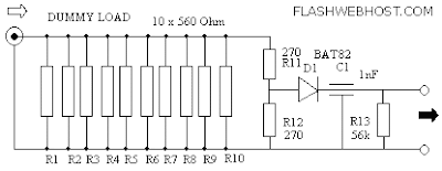
Phantom RF Dummy Load 10 Watts circuit Diagram


Phantom RF Load 10 Watts circuit Diagram


The circuit above is a dummy load capable of handling up to 10 watts of RF power for a few minutes, and its impedance is 50 ohms. It is constructed with 10 parallel resistors 560 ohms per 1 watt, R1 to R10, a voltage divider R11-R12 and a rectifier D1-C1. Its output voltage in a voltmeter which can be connected to measure the RF power.
Read More..

12V Step Down Dc Converter Using ADP2300 ADP2301

Using ADP2300 ADP2301 step-down dc dc regulators with integrated power MOSFET, can be designed a very simple DC DC voltage converter. Output voltage delivered by these circuits can be adjusted from 0.8 volts, up to 0.85xVin , with ±2% accuracy. The maximum output current that can be provided by ADP2300 ADP2301 regulators is up to 1.2 A load current.

12V Step-Down Dc Converter Circuit Diagram
12V Step-Down Dc-Converter-Circuit Diagram
12V Step-Down Dc-Converter-ADP2301
There are two frequency options: the ADP2300 runs at 700 kHz, and the ADP2301 runs at 1.4 MHz. These options allow users to make decisions based on the trade-off between efficiency and total solution size. Current-mode control provides fast and stable line and load transient performance.  Bellow you an see two design examples, which require few common electronic components.First circuit will provide a 2.5V output at a maximum current of 1.2A from an input voltage of 12 volts. Second circuit will provide a 5V output at a maximum current of 1.2A from an input voltage of 12 volts.
Read More..

Step Up Booster Powers Eight White LEDs

Tiny white LEDs are capable of delivering ample white light without the fragility problems and costs associated with fluorescent backlights. They do pose a problem however in that their forward voltage can be as high as 4 V, precluding them being from powered directly from a single Li-Ion cell. Applications requiring more white LEDs or higher efficiency can use an LT1615 boost converter to drive a series connected array of LEDs. The high efficiency circuit (about 80%) shown here can provide a constant-current drive for up to eight LEDs. Driving eight white LEDs in series requires at least 29 V at the output and this is possible thanks to the internal 36-V, 350-mA switch in the LT1615.

The constant-current design of the circuit guarantees a steady current through all LEDs, regardless of the forward voltage differences between them. Although this circuit was designed to operate from a single Li-Ion battery (2.5V to 4.5V), the LT1615 is also capable of operating from inputs as low as 1 V with relevant output power reductions. The Motorola MBR0520 surface mount Schottky diode (0.5 A 20 V) is a good choice for D1 if the output voltage does not exceed 20 V. In this application however, it is better to use a diode that can withstand higher voltages like the MBR0540 (0.5 A, 40 V). Schottky diodes, with their low forward voltage drop and fast switching speed, are the best match.

Many different manufacturers make equivalent parts, but make sure that the component is rated to handle at least 0.35 A. Inductor L1, a 4.7-µH choke, is available from Murata, Sumida, Coilcraft, etc. In order to maintain the constant off-time (0.4 ms) control scheme of the LT1615, the on-chip power switch is turned off only after the 350-mA (or 100-mA for the LT1615-1) current limit is reached. There is a 100-ns delay between the time when the current limit is reached and when the switch actually turns off. During this delay, the inductor current exceeds the current limit by a small amount. This current overshoot can be beneficial as it helps increase the amount of available output current for smaller inductor values.


This will be the peak current passed by the inductor (and the diode) during normal operation. Although it is internally current-limited to 350 mA, the power switch of the LT1615 can handle larger currents without problems, but the overall efficiency will suffer. Best results will be o btained when IPEAK is kept well below 700 mA for the LT1615.The LT1615 uses a constant off-time control scheme to provide high efficiencies over a wide range of output current. The LT1615 also contains circuitry to provide protection during start-up and under short-circuit conditions.

When the FB pin voltage is at less than approximately 600 mV, the switch off-time is increased to 1.5 ms and the current limit is reduced to around 250 mA (i.e., 70% of its normal value). This reduces the average inductor current and helps minimize the power dissipation in the LT1615 power switch and in the external inductor L1 and diode D1. The output current is determined by Vref/R1, in this case, 1.23V/68 = 18 mA). Further information on the LT1615 may be found in the device datasheets which may be downloaded from www.linear-tech.com/pdf/16151fa.pdf

 
Author: D. Prabakaran
Read More..

12 V Bidirectional Motor Control Circuit

This simple circuit drives DC motors with a maximum current of 1 A and can be built with readily available components.The output voltage is adjustable between 0 and 14 V and the polarity can be changed so that not only motor speed but also rotation direction can be adjusted by turning a knob. 

The circuit is also ideal as a controller for a DC model railway or small low voltage hobby tool. Power for the circuit is supplied by a 18 V mains transformer rated at 1.5 A. Diodes D1to D4 rectify the supply and capacitor C1 provides smoothing to give a DC output voltage of around 24 V. A classic ‘H’ bridge configuration is made up with transistors T1/T3 and T2/T4. Transistors T5 and T6 together with resistors R7 and R8 provide the current sense and limiting mechanism. The maximum output current limit can be changed from 1 A by using different value resistors for R7 and R8: IOUT = 0.6 V / R where R gives the value for R7 and R8. For increased current limit the mains transformer and diodes will need to be changed to cope with the extra current as well as the four transistors used in the bridge configuration. 

Circuit diagram:
12 V Bidirectional Motor Control Circuit Diagram  12 V Bidirectional Motor Control Circuit Diagram
 
Motor speed control and direction is controlled by a twin-ganged linear pot (P1). The two tracks of P1 together with R1/R2 and R3/R4 form two adjustable potential divider networks. Wiring to the track ends are reversed so that as the pot is turned the output voltage of one potential divider increases while the other decreases and vice versa. 

In the midway position both dividers are at the same voltage so there is no potential difference and the motor is stationary. As the pot is rotated the potential difference across the motor increases and it runs faster. The voltage drop across D5 and D6 is equal to the forward voltage drop VBE of the bridge transistors and ensures that the motor does not oscillate in the off position with the pot at its mid point.


http://www.ecircuitslab.com/2011/07/12-v-bidirectional-motor-control.html
Read More..