Showing posts with label simple. Show all posts

Tuesday, November 11, 2014

Simple Solar Tracking System

Generally, solar panels are stationary and do not follow the movement of the sun. Here is a solar tracker system that tracks the sun’s movement across the sky and tries to maintain the solar panel perpendicular to the sun’s rays, ensuring that the maximum amount of sunlight is incident on the panel throughout the day. The solar tracker starts following the sun right from dawn, throughout the day till evening, and starts all over again from the dawn next day. 

Fig. 1: Circuit of solar tracking system
 

Fig. 1 shows the circuit of the solar tracking system. The solar tracker comprises comparator IC LM339, H-bridge motor driver IC L293D (IC2) and a few discrete components. Light-dependent resistors LDR1 through LDR4 are used as sensors to detect the panel’s position relative to the sun. These provide the signal to motor driver IC2 to move the solar panel in the sun’s direction. LDR1 and LDR2 are fixed at the edges of the solar panel along the X axis, and connected to comparators A1 and A2, respectively. Presets VR1 and VR2 are set to get low comparator output at pins 2 and 1 of comparators A1 and A2, respectively, so as to stop motor M1 when the sun’s rays are perpendicular to the solar panel.

When LDR2 receives more light than LDR1, it offers lower resistance than LDR1, providing a high input to comparators A1 and A2 at pins 4 and 7, respectively. As a result, output pin 1 of comparator A2 goes high to rotate motor M1 in one direction (say, anti-clockwise) and turn the solar panel.

When LDR1 receives more light than LDR2, it offers lower resistance than LDR2, giving a low input to comparators A1 and A2 at pins 4 and 7, respectively. As the voltage at pin 5 of comparator A1 is now higher than the voltage at its pin 4, its output pin 2 goes high. As a result, motor M1 rotates in the opposite direction (say, clock-wise) and the solar panel turns.
 

Fig. 2 Proposed assembly for the solar tracking system
 
Similarly, LDR3 and LDR4 track the sun along Y axis. Fig. 2 shows the proposed assembly for the solar tracking system.

Read More..

Wednesday, November 5, 2014

Simple Door Alarm

This circuit emits a beep and/or illuminates a LED when someone touches the door-handle from the outside. The alarm will sound until the circuit will be switched-off.  The entire circuit is enclosed in a small plastic or wooden box and should be hanged-up to the door-handle by means of a thick wire hook protruding from the top of the case.
 
A wide-range sensitivity control allows the use of the Door Alarm over a wide variety of door types, handles and locks. The device has proven reliable even when part of the lock comes in contact with the wall (bricks, stones, reinforced concrete), but does not work with all-metal doors. The LED is very useful during setup.
Door Alarm Circuit diagram:
Alarm 
Parts:
R1______________1M 1/4W Resistor
R2______________3K3 1 or 2W Resistor (See Notes)
R3_____________10K 1/2W Trimmer Cermet (See Notes)
R4_____________33K 1/4W Resistor
R5____________150K 1/4W Resistor
R6______________2K2 1/4W Resistor
R7_____________22K 1/4W Resistor
R8______________4K7 1/4W Resistor

C1,C2__________10nF 63V Ceramic or Polyester Capacitors
C3_____________10pF 63V Ceramic Capacitor
C4,C6_________100nF 63V Ceramic or Polyester Capacitors
C5______________2µ2 25V Electrolytic Capacitor
C7____________100µF 25V Electrolytic Capacitor


D1,D2,D4_____1N4148 75V 150mA Diodes
D3_____________5 or 3mm. Red LED

Q1,Q2,Q3,Q5___BC547 45V 100mA NPN Transistors
Q4____________BC557 45V 100mA PNP Transistor

L1_________________ (See Notes)
L2_____________10mH miniature Inductor

Hook_______________ (See Notes)

BZ1___________Piezo sounder (incorporating 3KHz oscillator)

SW1,SW2________SPST miniature Slider Switches

B1_______________9V PP3 Battery

Clip for PP3 Battery

Circuit operation:

Q1 forms a free-running oscillator: its output bursts drive Q2 into saturation, so Q3 and the LED are off. When part of a human body comes in contact with a metal handle electrically connected to the wire hook, the body capacitance damps Q1 oscillations, Q2 biasing falls off and the transistor becomes non conducting. Therefore, current can flow into Q3 base and D3 illuminates. If SW1 is closed, a self-latching circuit formed by Q4 & Q5 is triggered and the beeper BZ1 is activated.

When the human body part leaves the handle, the LED switches-off but the beeper continues to sound, due to the self-latching behavior of Q4 & Q5. To stop the beeper action, the entire circuit must be switched-off opening SW2. R3 is the sensitivity control, allowing to cope with a wide variety of door types, handles and locks.

Notes:
  • L1 is formed winding 20 to 30 turns of 0.4mm. diameter enameled copper wire on R2 body and soldering the coil ends to the resistor leads. You should fill R2 body completely with coil winding: the final turns number can vary slightly, depending on different 1 or 2W resistor types actual length (mean dimensions for these components are 13 - 18mm. length and 5 - 6mm. diameter).
  • The hook is made from non-insulated wire 1 - 2mm. diameter (brass is well suited). Its length can vary from about 5 to 10cm. (not critical).
  • If the device is moved frequently to different doors, Trimmer R3 can be substituted by a common linear potentiometer fitted with outer knob for easy setup.
  • To setup the device hang-up the hook to the door-handle (with the door closed), open SW1 and switch-on the circuit. Adjust R3 until the LED illuminates, then turn slowly backwards the screwdriver (or the knob) until the LED is completely off. At this point, touching the door-handle with your hand the LED should illuminate, going off when the hand is withdrawn. Finally, close SW1 and the beeper will sound when the door-handle will be touched again, but will not stop until SW2 is opened.
  • In regular use, it is advisable to hang-up and power-on the device with SW1 open: when all is well settled, SW1 can be closed. This precautionary measure is necessary to avoid unwanted triggering of the beeper.

Read More..

Tuesday, November 4, 2014

Simple Detector with Amplification

A simple shortwave radio detector is neither very sensitive nor very selective. However, with a little extra amplification we can improve the reception performance significantly.

The additional circuit is designed to compensate for the losses in the resonant circuit. A transistor is used to amplify the RF signal and feed it back into the resonant circuit. When the gain is set correctly we can make the amount of this feedback exactly equal to the losses. The resonant circuit is then critically damped and has a very high Qfactor. Now we can separate transmissions that are just 10 kHz apart, and we can tune in to very weak stations.

Detector with Amplification Circuit Diagram :


Amplification-Circuit

The tuning capacitor used has two gangs of vanes with capacitances of 240 pF and 80 pF. These two gangs are connected in parallel to make a 320 pF variable capacitance. The air-cored inductor has 25 turns on a diameter of 10 mm, with taps at 5-turn intervals. The resonant circuit so formed is capable of covering the full shortwave  band from 5 MHz to 25 MHz.

The short wave detector can be connected to a power amplifier, or, for exam-ple, amplified PC loudspeakers. The antenna does not have to  be very long: in experiments we used a one metre length of wire. Tuning the radio involves adjusting the variable capacitor to bring in the station and then adjusting the gain of the feed-back circuit for optimal output volume. If the potentiometer is turned up too far, the receiver will go into self-oscillation and become a mini-transmitter. At  the optimal setting the sound  quality is very pleasant and certainly no worse than many ordinary shortwave radios.

If you find shortwave detectors that use a battery and an amplifier a little new-fangled, you can get your fix of nostalgia by dispensing with the battery and connecting a crystal earpiece to the detector’s output. The radio will of course also work without the feedback circuit, but with rather poorer performance.


Read More..

Tuesday, October 28, 2014

Simple 150 Watt Power Amplifier Circuit

This is the very simple circuit diagram of 150W power amplifier. The circuit is easy enough to built without PCB. The power output range is about 100-150W depends to the power supply and the Darlington’s you use for the amplifier. Heatsink is a must since the final transistor is going to hot when the amplifier is activated.

Simple


The amplifier requires split power supply. The transformer is depending to your home electrical installation, it can be 110V or 220V primary. Use 35V-0-35V secondary (transformer output), you will get about 45V DC output from transformer 35V AC after rectified by the diodes. The Transformer current output should be at least 4A for better audio performance. Use 4A / 100V diodes.
Read More..

Sunday, October 26, 2014

LA4460 Simple Audio Amplifier

A unpretentious audio amplifier circuit can happen designed using the LA4460 IC . This circuit is very simple and require little exterior electronic components . The LA4460 IC is in fact used on behalf of car broadcasting or else car audio power amplifier and could provide output power up to 12 W. But at home this circuit is solitary used 5W.
LA4460 Audio Amplifier Circuit
This amplifier circuit can come about used for car means of communication applications , small screen , or else around other audio circuits so as to don’t require vast power .
explanation:
  1. work 12VDC to supply the circuit.
  2. Mount the LA4460 IC  with an appropriate high temperature sink
  3. Some of as a rule worthy skin of the LA4460 IC are : reverse connection protection , muting function,thermal runaway protection circuit ,completed voltage & pitch voltage protection circuit, load stunted-circuit current limiting protection circuit, output pins DC short-circuit protection.
Read More..

Thursday, October 23, 2014

Simple 5V Regulated Power Supply Circuit Diagram

5V Regulated Power Supply Circuit Diagram is a small +5V power supply, which is useful when experimenting with digital electronics. Small inexpensive wall tranformers with variable output voltage are available from any electronics shop and supermarket. Those transformers are easily available, but usually their voltage regulation is very poor, which makes then not very usable for digital circuit experimenter unless a better regulation can be achieved in some way.

The following circuit is the answer to the problem. This circuit can give +5V output at about 150 mA current, but it can be increased to 1 A when good cooling is added to 7805 regulator chip. The circuit has overload and thermal protection. The capacitors must have enough high voltage rating to safely handle the input voltage feed to circuit. The circuit is very easy to build for example into a piece of veroboard.

 5V Regulated Power Supply Circuit Diagram
Parts:

C1 = 100uF-25V electrolytic capacitor, at least 25V voltage rating
C2 = 10uF-25V electrolytic capacitor, at least 6-16V voltage rating
C3 = 100nF-63V ceramic or polyester capacitor
IC = 7805 regulator IC

ICs Pinout :
  1. Unregulated voltage in
  2. Ground (See Diagram)
  3. Regulated voltage out

Circuit features:
  • Gives out well regulated +5V output, output current capability of 100 mA
  • Built-in overheating protection shuts down output when regulator IC gets too hot
  • Very simple and easy to build
  • Very stable +5V output voltage, reliable operation
  • Easy to get components, uses only very common basic components
  • Based on datasheet example circuit, I have used this circuit succesfully as part of many electronics projects
  • Part of electronics devices, small laboratory power supply
  • Wide range of input unreglated DC 8-24V power supply
  • Few dollars for the electronics components + the input transformer cost

Modification Iideas

More output current:

If you need more than 150 mA of output current, you can update the output current up to 1A doing the following modifications.
  • Change the transformer from where you take the power to the circuit to a model which can give as much current as you need from output
  • Put a heatsink to the 7805 regulator (so big that it does not overheat because of the extra losses in the regulator)

More output voltages:

If you need other voltages than +5V, you can modify the circuit by replacing the 7805 chips with another regulator with different output voltage from regulator 78xx chip family. The last numbers in the the chip code tells the output voltage. Remember that the input voltage muts be at least 3V greater than regulator output voltage ot otherwise the regulator does not work well.

Read More..

Wednesday, October 22, 2014

Simple Purpose Alarm

The alarm may be used for a variety of applications, such as frost monitor, room temperature monitor, and so on. In the quiescent state, the circuit draws a current of only a few microamperes, so that, in theory at least, a 9 V dry battery (PP3, 6AM6, MN1604, 6LR61) should last for up to ten years. Such a tiny current is not possible when ICs are used, and the circuit is therefore a discrete design. Every four seconds a measuring bridge, which actuates a Schmitt trigger, is switched on for 150 ms by a clock generator. In that period of 150 ms, the resistance of an NTC thermistor, R11, is compared with that of a fixed resistor. If the former is less than the latter, the alarm is set off.

When the circuit is switched on, capacitor C1 is not charged and transistors T1–T3 are off. After switch-on, C1 is charged gradually via R1, R7, and R8, until the base voltage of T1 exceeds the threshold bias. Transistor T1 then comes on and causes T2 and T3 to conduct also. Thereupon, C1 is charged via current source T1-T2-D1, until the current from the source becomes smaller than that flowing through R3 and T3 (about 3 µA). This results in T1 switching off, so that, owing to the coupling with C1, the entire circuit is disabled. Capacitor C1 is (almost) fully charged, so that the anode potential of D1 drops well below 0 V. Only when C1 is charged again can a new cycle begin.


It is obvious that the larger part of the current is used for charging C1. Gate IC1a functions as impedance inverter and feedback stage, and regularly switches on measurement bridge R9–R12-C2-P1 briefly. The bridge is terminated in a differential amplifier, which, in spite of the tiny current (and the consequent small transconductance of the transistors) provides a large amplification and, therefore, a high sensitivity. Resistors R13 and R15 provide through a kind of hysteresis a Schmitt trigger input for the differential amplifier, which results in unambiguous and fast measurement results. Capacitor C2 compensates for the capacitive effect of long cables between sensor and circuit and so prevents false alarms.

If the sensor (R11) is built in the same enclosure as the remainder of the circuit (as, for instance, in a room temperature monitor), C2 and R13 may be omitted. In that case,C3 willabsorb any interference signals and so prevent false alarms. To prevent any residual charge in C3 causing a false alarm when the bridge is in equilibrium, the capacitor is discharged rapidly via D2 when this happens. Gates IC1c and IC1d form an oscillator to drive the buzzer (an a.c. type). Owing to the very high impedance of the clock, an epoxy resin (not pertinax) board must be used for building the alarm. For the same reason, C1 should be a type with very low leakage current. If operation of the alarm is required when the resistance of R11 is higher than that of the fixed resistor, reverse the connections of the elements of the bridge and thus effectively the inverting and non-inverting inputs of the differential amplifier.

An NTC thermistor such as R11 has a resistance at –18 °C that is about ten times as high as that at room temperature. It is, therefore, advisable, if not a must, when precise operation is required, to consult the data sheet of the device or take a number of test readings. For the present circuit, the resistance at –18 °C must be 300–400 kΩ. The value of R12 should be the same. Preset P1 provides fine adjustment of the response threshold. Note that although the prototype uses an NTC thermistor, a different kind of sensor may also be used, provided its electrical specification is known and suits the present circuit.


Author: K. Syttkus
Copyright: Elektor Electronics


Read More..

Simple Meter Impedance Speaker Circuit Diagram

A simple impedance meter can be useful to measure the actual impedance of a speaker or headset, ideal for anyone working with sound, making and repairing speakers. This impedance meter works in conjunction with a multimeter or oscilloscope to measure the impedance.

Meter Impedance Speaker Circuit Diagram

Meter Impedance Speaker Circuit Diagram


How to make the measurement of impedance speaker with the multimeter

Connect a digital multimeter to AC voltage in the range of 200mV.
Connect the device under test terminals
SW1 to R7, if the value of the measured impedance is less than 100 ohm R8 or upwards.
With SW2 in the "Set" power-on circuit through SW3
Adjust P1 to read exactly 100.0mV the display DVM
Switch SW2 in the "Measure" and read directly from the speaker or headphones impedance value on the display DVM, eg 8.2mV = 8.2 Ohm / 80.1mV = 80.1 Ohm


How to make the measurement of impedance speaker with the oscilloscope:

Connect the oscilloscope instead of DVM (multimeter) and turn P1 fully clockwise.
Short the output speaker and adjust R3 to get a sine wave amplitude of about 2.2V peak-to-peak.
How to make the impedance measurement Speaker "By ear"

Connect a small speaker or headphones, forming a pair of headphones to the output of the circuit and turn P1 to obtain a level of sound output moderated. Carefully adjust R3 until the output sound stops, then turn the trimpot to adjust slowly and stop immediately when the sound start again.

List of components


P1 4K7 linear potentiometer
R1 12K 1/4W Resistor
R2 2K2 1/4W Resistor
R3 1K 1/2W Trimmer (cermet)
R4 1K5 1/4W Resistor
4K7 1/4W Resistor R5
R6 3K3 1/4W Resistor
R7 100R 1/4W Resistor (See Notes)
R8 1K 1/4W Resistor (See Notes)
R9 1K 1/4W Resistor (Optional)
22NF 63V Polyester Capacitor C1
C2 330nF 63V Polyester Capacitor
C3 22μF 25V Electrolytic Capacitor
D1, D2 1N4148 75V 150mA Diodes
D3 3mm red LED (Optional)
Q1, Q2, Q3 BC550C 45V 100mA Low noise High gain NPN
IC1 78L05 5V 100mA Regulator IC
SW1, SW2 SPDT Toggle or Slider
SW3 SPST switch or Slider
B1 9V PP3 battery for PP3Clip

Notes:

For very precise measurements using resistors R7 and R8 with 1% or 2% tolerance.
D3 LED pilot and his current limiting resistor R9 are optional.
Read More..

Monday, October 20, 2014

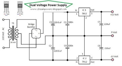
Simple Dual Voltage Power Supply 12 Volt

This is the simple circuit diagram of Dual Voltage Power Supply. It is used for Misc… application. This circuit is called regulated power supply. For this reason the main component of this circuit is Regulator IC. It also needs few components to built. The regulator 7812 is the positive voltage regulator and 7912 is the negative voltage regulator. 

Simple Dual Voltage Power Supply 12 Volt


You can also use 7809 for 9 volt positive power supply and 7909 for negative voltage power supply. It regulates voltage from 24Volt to 12 Volt (DC). The transformer input is 110Volt to 220Volt (AC) and the output must be between 12Volt to 24Volt (AC) and current must be 500mA. In this circuit some capacitors are used as a filter for removing repole.
Read More..

Thursday, October 16, 2014

Simple Automatic Water Pump Controller Circuit Diagram

Simple Automatic Water Pump Controller Circuit Diagram is a series of functions to control the Automatic Water Pump Controller Circuit in a reservoir or water storage. As the water level sensor made with a metal plate mounted on the reservoir or water tank, with a sensor in the short to create the top level and a detection sensor for detecting long again made the lower level and ground lines connected to the bottom of reservoirs or reservoir. 

The series of automatic water pump controller is designed with 2 inputs NOR by 4 pieces and relay that is activated by the transistor. Automatic water pump circuit requires +12 VDC voltage source and can be used to control the water pump is connected to AC power . Here is the complete series of pictures.

Automatic Water Pump Controller Circuit Diagram


working principle series of automatic water pump controller above is. At the time the water level is below both sensors, the output IC1C (pin 10) will be LOW, Kemudin when the water began to touch the lower level sensor, the output IC1C (pin10) remains LOW until the water touches the sensor level above, then the output IC1C (pin 10) going HIGH and active relay through Q1 and turn on the water pump to meguras reservoir. 

At the muli down and water level sensors for water untouched MKA IC1C output (pin 10) remains HIGH until the new water untouched semuasensor IC1C output (pin 10) LOW and water pump died. The series of automatic water pump controller is equipped with SW1 which serves to reverse the logic of drains (the output of IC1C) and the concept of water supplied (output dri IC1D). 

When SW1 is connected to IC1D the water pump will turn on when the water does not touch all the sensors and will die when all the sensors tesentuh water. Automatic water pump controller can be used to fill or drain the water according to which mode is selected via SW1.

List Component Automatic Water Pump Controller
R1 = 15K
R2 = 15K
R3 = 10K
R4 = 1K
D1 = LED
D2 = 1N4148
Q1 = BC337
IC1 = 4001
SW = SPDT Switches
Relay RL1 = 12V

Read More..

Simple Smoggy Circuit Schematic

Even if your good old (Sony) Walkman  sees little use nowadays it would be a  shame to get rid of it altogether. The more  so when just removing the tape head  would allow the built-in audio amplifier  to become an outstanding electrosmog  detector for a variety of purposes. Looking at the schematic, readers with RF  experience will have no difficulty in recognising the diodes and coils of the two  detector-receivers, which serve to capture and demodulate RF signals. With its  coil of four turns (L2) one receiver covers the higher frequency range of the  electromagnetic waves, whilst the sec-ond detector takes care of the lower frequency range. 

Circuit diagram :
Simple Smoggy-Circuit Schematic
Simple Smoggy Circuit Diagram

For this reason a coil with a  greater number of turns is required: L1 is  an RF choke of about 250 µH. The precise  value is not critical and it could equally be  220 µH or 330 µH. The outputs of both detector-receivers  are connected to the cables disconnected  previously from the tape heads, feeding the  right and left channel inputs to the Walk-man’s audio amplifier. Please note here that  the screening of the tape head cable does not  have to be absolutely identical to the ground connection of the amplifier circuitry. As  we are dealing with a stereo amplifier,  we are listening into both channels and  thus both RF ranges at the same time.
One channel of the amplifier can also be  used to demodulate low-frequency magnetic alternating fields  via a capacitor  (C3) bypassing diode D1 and connecting either a third coil (L3, for instance;  a telephone recording adapter) as the  pickup device or else a long piece of wire  for acquiring low frequency AC electrical fields. Sources like this are discernible mainly by a distinct 50 Hz (or 60 Hz)  humming in the earphones. Predicting what you may hear down to  the very last detail is difficult, since every  locality has its own, individual interference sources. Nevertheless, with practice  users will succeed in identifying these  interference sources by their particular  audio characteristics. 

To sum up, four different ‘sensors’ can be  connected to the inputs of this circuit:  ANT1 (approx. 50 cm long whip antenna),  ANT2 (3.5 cm short stub antenna), ANT3  (approx. 1 m long wire antenna for low frequency electrical fields) and a coil for magnetic fields. Finally, two more tips:
  1. Use only ‘good old’ germanium diodes for  D1 and D2. Sensitivity will be much reduced if  silicon diodes are used, as these have a higher  threshold voltage.
  2. Smoggy does not provide an absolute indi-cation of field strength and even more so can-not provide any guidance whether anything  it detects might be harmful. Its function is to detect electromagnetic signals and compare  their relative magnitude.
Author : Tony Ruepp  - Copyright : Elektor
Read More..

Simple HiFi Expandor Circuit Diagram with De emphasis

This is the schematic design of HiFi Expandor Circuit with De-emphasis. The circuit is based NE570. The NE570 can be used to construct a high performance compandor suitable for use with music. This type of system can be used for noise reduction in tape recorders, transmission systems, bucket brigade delay lines, and digital audio systems. The circuits to be described contain features which improve performance, but are not required for all applications.

 HiFi Expandor Circuit  Diagram 

The expandor to complement the compressor is shown in the above circuit. Here an external op amp is used for high slew rate. Both the compressor and expandor have unity gain levels of 0dB. Trim networks are shown for distortion (THD) and DC shift. The distortion trim should be done first, with an input of 0dB at 10kHz. The DC shift should be adjusted for minimum envelope bounce with tone bursts. When applied to consumer tape recorders, the subjective performance of this system is excellent.
Read More..

Wednesday, October 15, 2014

Simple Chip Divider Circuit Diagram

We can build a divider circuit using only a single chip component, a special purpose integrated circuit AD532. We can configure the AD532 as a two quadrant divider by connecting the multiplier cell in the feedback loop of the op amp and using the Z terminal as a signal input, as shown in the following figure. For your note, the output error is given approximately by 10 Vεm/ (X1-X2), where εm is the total error specification for the multiply mode and bandwidth by fm x (X1-X2)/10 V, where fm is the bandwidth of the multiplier. 

The X input is restricted to negative values to avoid positive feedback. Thus, connect the input to X and the offset null to X2 for single ended negative inputs. For single ended positive inputs (0V to +10V), connect the input to X2 and the offset null to X1. Gain (S.F) and offset (X0) adjustment are recommended as shown and explained in the following table for optimum performance. The useful range in denominator input is approximately 500 mV ≤ (X1-X2) ≤ 10 V for practical reason. If used, the voltage offset adjust (Vos) is trimmed with Z at zero and (X1-X2) at full scale.

 Simple Chip Divider Circuit Diagram


Read More..

Thursday, October 2, 2014

Simple Hobby Circuits

10 OUTPUT LED SEQUENCERHere is 10 output LED sequencer. After the last LED is illuminated, the circuit is reset. This circuit is build around readily available, low cost components - a 555 and decade counter CD4O1 7. The timer IC NE555 is wired as an astable multivibrator that produces 6Hz clock at its output pin 3. The 4017 is a CMOS decade counter with 10 outputs. Inputs include a CLOCK (Pin 1 4), a RESET (Pin 15), and a CLOCK INHIBIT (Pin 13). The clock input connects to a Schmitt trigger for pulse shaping and allows slow clock rise and fall times (not needed in our case).

The counter advances one output at the rising edge of the clock signal if the CLOCK INHIBIT line is low. A high RESET signal resets the counter to the zero output. The circuit may be configured for counts less than 10 by connecting RESET to an output pin (one after the desired count). Thus, a five stage sequencer can be made by connecting pin 15 to pin 1. A CARRY-OUT signal (pin 12) can be used to clock subsequent stages in a multi-device counting chain.

The output from 1C2 pin 3 is connected to clock pin (pin 14) of the IC3 for sequencing operations. NPN transistors Q1- Q10 are used to increase the output current for the LEDs which is set by the common 150 ohm resistor. In the circuit, only one of the outputs is HIGH at any one time and the output advances by one count with every clock pulse.
But the circuit above is poorly designed.
It does not need the voltage regulator as both chips can work up to 15v.
The 4017 can supply 10mA to a LED on a 12v supply so that none of the transistors are needed.
The circuit below shows the necessary components.
The secret to designing a circuit is to look at the final design and ask: "is this component necessary?"
Try removing a component and see if the circuit still works. Keep doing this with all the components. The circuit above was published in an Indian magazine with over 1,000,000 readers. The faults were obvious. How these faults passed an editorial committee is beyond me. They are showing very poor design-leadership in allowing this oversight to be published. The faults are technical but are obvious to anyone who has constructed the circuit and experimented with it. Obviously the circuit has never been assembled with anyone with technical expertise.

to Index


12v LAMP DIMMER
Here is a 12 volt @ 2 amp lamp dimmer that can be used to dim a standard 25 watt bulb by controlling the duty cycle of a astable 555 timer oscillator. When the potentiometer is at the up position, the capacitor will charge quickly through both 1k resistors and the diode, producing a short positive interval and long negative interval which dims the lamp to near darkness. When the potentiometer is at the lower position, the capacitor will charge through both 1k resistors and the 50k potentiometer and discharge through the lower 1k resistor, producing a long positive interval and short negative interval which brightens the lamp to near full intensity. The duty cycle of the 200Hz square wave can be varied from approximately 5% to 95%. The two circuits below show how to connect the lamp to either the positive or negative side of the supply.
But the first circuit has a mistake and some components are not needed. The 555 will sink 300mA and it can be connected directly to the output transistor - you dont need the buffer transistor.
When the 555 goes HIGH, the voltage on Pin 3 is 1.5v lower than the 12v rail and thus the transistor does not turn off. The two diodes in the circuit below are needed to drop an additional 1v so the transistor turns off.

to Index


16-LED NIGHT RIDER
The bi-directional sequencer uses a 4 bit binary up/down counter (CD4516) and two “1 of 8 line decoders" (74HC138 or 74HCT138) to generate the popular Night Rider display. A Schmitt Trigger oscillator provides the clock signal for the counter and the rate can be adjusted with the 500k pot. Two additional Schmitt Trigger inverters are used as a SET/RESET latch to control the counting direction (up or down). Be sure to use the 74HC14 and not the 74HCT14, the 74HCT14 may not work due to the low TTL input trigger level. When the highest count is reached (1111) the low output at pin 7 sets the latch so that the UP/DOWN input to the counter goes low and causes the counter to begin decrementing. When the lowest count is reached (0000) the latch is reset (high) so that the counter will begin incrementing on the next rising clock edge. The three lowest counter bits (Q0, Q1, Q2) are connected to both decoders in parallel and the highest bit Q3 is used to select the appropriate decoder.
to Index


555 SCHMITT
The popular NE555 is used as a Schmitt trigger by connecting Pin 2 and threshold pin 6 inputs.
As the light falling on the LDR falls below a preset value the relay energises. This happens when the voltage at pin 2,6 is greater than 2/3 of Vcc. When light increases, the voltage at pin 2,6 falls and at 1/3 of Vcc the relay is de-energised. This gives a Hysteresis range. Diode IN 4001 is necessary for the
safety of the IC.

to Index


CONSTANT CURRENT SOURCE
In the following circuit an LED is used to give a fixed reference voltage to a transistor. The output constant current I out is given by:
The LED lights up only when a load is connected at the output. Thus it indicates when the circuit is operating.
The operation of the circuit can be made clearer by re-arranging the components as follows:

The output will be limited to 100mA by using a red LED and 10R for Re.
The output will be limited to 500mA by using a red LED and 2R2 for Re.
The output will be limited to 1A by using a red LED and 1R0 for Re.
to Index


AC DETECTOR
This circuit will detect AC line currents of about 250mA or more without making any electrical connections to the line. Current is detected by passing on of the AC lines through an inductive pickup (L1) made with a 1 inch diameter U-bolt wound with 800 turns of #35 magnet wire. The pickup can be made from other iron type rings or transformer cores that allows enough space to pass one of the AC lines through the center. Only one of the current carrying lines, either the line or the neutral should be put through the center of the pickup to avoid the fields cancelling.
This is most important is very difficult to achieve. The best method is to make a short extension cord with the three conductors separated from each other.
If you make a 3-turn loop with say the active line, and pass a straight rod such as a metal bolt, containing 400 or more turns through the centre of the 3-turns, you will produce a very sensitive pick-up.
The magnetic pickup produces about 4 millivolts for AC line current of 250mA, or AC load of around 30 watts. The signal from the pickup is increased about 200 times at the output of the op-amp pin 7 which is then peak detected by the capacitor and diode connected to pin 7. The second op-amp is used as a comparator which detects a voltage rise greater than the diode drop. The minimum signal
needed to cause the comparator stage output to switch positive is around 800mV which corresponds to about a 30 watt load on the AC line. The output of the 1458 op-amp will only swing within a couple volts of ground so a voltage divider (1k/470) is used to reduce the no signal voltage to about 0.7 volts. An additional diode is added in series with the transistor base to ensure it turns off when the op-amp voltage is 2 volts. You may get a little bit of relay chatter if the AC load is close to the switching point so a larger load of 50 watts or more is recommended. The sensitivity can be increased by adding more turns to the pickup.
to Index


AUTO CUTOUT
A 12v relay is connected across the 12v supply. When the output is shorted, the 12v falls to 0v and the relay drops-out. The contacts open the 12v is reapplied to the relay and it will "chatter" if the short is not removed.
This circuit will simply not work and the relay will simply become a "Buzzer."


In the following circuit, the transistor will only turn on if the output voltage is above 0.6v.
to Index


DOOR WATCHER
Three reed switches are at the heart of the circuit, one fitted to each door. They close when a door is opened. An associated LED lights when a door is opened.
The remainder of the circuit is powered by either D1, D2 or D3. However the 555 is not enabled until pin 4 goes high and this requires the output of either IC1a or IC1b to go high. In turn, this requires either pin 1 ,2 or 4 go high and this happens when a door opens. Because the high on each pin is only momentary (i.e. about 1/3 second, while C1 ,C2 or C3 is charging) there is only a short burst of buzzer activity (two brief beeps) at each door opening, after which it goes mute again.
So the beep calls attention to the fact that a door has opened and the LED indicates which door, staying lit until [i door is closed. If another door opens before the first door is closed, there is another beep and another LED lights.

The circuit above is too complex. It is very poorly designed. The 3 signals diodes are doing NOTHING. The are simply across each other!! One diode could be placed in the supply line to the 555 if it is needed for the reset line to work correctly. R7 is not needed as the output is taken to the pins 2&6 and the 74LS32 chip can be replaced by 3 x 470u electrolytics.
It can be simplified to this:

to Index


EMERGENCY LIGHT
Here is a circuit of an emergency light. As long as the power supply is present, transistor Q1 conducts. Since the base of the transistor Q2 is connected to the collector of Q1, transistor Q2 and Q3 do not conduct and hence the lamp remains off. LED glows as long as the supply is present.
When the power supply fails, the base drive to Q1 disappears. Thus Q1 stops conducting and its collector voltage jumps to battery voltage and starts conducting, switching on the lamp instantly. The load current is supplied by the battery. Whenever the power supply is restored, Q1 starts conducting turning Q2 & Q3 off and the lamp is switched off. Transistor Q2 conducts and provides sufficient base drive to transistor Q3.
The circuit above is too complex. The first diode is not needed and the rest of the circuit can be re-arranged. The 2R2 will overcharge the battery and dry it out in a few months.
It can be simplified to this:

The 100R gives 40mA charging with a 12v battery and 12v DC plug pack.
to Index


INCREASING THE INPUT IMPEDANCEThe input impedance of a low cost analogue multimeter can be improved using this circuit. The approximate impedance increase will be about 250.
The LED provides a fixed reference voltage for zero setting of the multimeter via VR1.

to Index


BATTERY MONITOR
This circuit makes it possible to monitor the charging process of a battery. After constructing the circuit, final adjustments are simple and the only thing needed is a digital voltmeter for the necessary accuracy. Connect an input voltage of 12.65 volt between the positive and negative connections of the circuit and adjust the VR1 (10K trimmer) until Led 10 lights up. Lower the voltage and in sequence all other LEDs will light up. Check that Led 1 lights up at approximately 11.85 volts. At 12.65 volt and higher the battery is fully charged, and at 11.85 is considered to be at its lowest state. LED 8, 9 and 10 indicate the battery capacity is more than 50%, LED 4 to LED 7 indicate a capacity of 30% - 50% and LED 1 to LED 3 indicate less that 30%. This circuit, with the components shown, uses less than 10mA. Of course you can adapt it to your own needs by making small modifications. This circuit is set for DOT mode, meaning only one LED at a time will be lit. If you wish to use the BAR mode, connect pin 9 to the positive supply rail, but obviously with increased current consumption. The LED brightness can be adjusted by choosing a different value for the 5k6 resistor connected at pin 6 and 7. The diode 1N4007 was included to protect the circuit from a wrong polarity connection.
to Index


CAPACITANCE BEEPERHere is a circuit of capacitance beeper which uses a two-transistor flasher in conjunction with a Darlington transistor. When the probe is touched to a capacitor, the project beeps at a frequency that varies with capacitance. The frequency change is so noticeable that small capacitors can be precisely matched or an exact fixed value can be selected to replace a trimmer in a prototype.
When the beeper is properly adjusted it draws only 10uA with nothing touching the probe excluding the LED current. This design is optimized for capacitors less than about 100n. Large capacitors give a low frequency clicking sound and small capacitors sound a tone that increases as the capacitance decreases. Many decades of frequency change occur over the beepers range.
The probe should be built into a metal box so that one hand makes good
contact to 0v.
The resistor values are selected to barely turn on the transistors to conserve battery power. The transistors must have very high gain and good low current properties. The MPS-A18 is a very high gain transistor with excellent gain at very low currents. The capacitors are not particularly critical but the trimmer might require a little care. The trimmer is adjusted until the beeping just stops and only a very weak squeal is heard when a 2.2p is touched to the probe.
to Index


LIGHT CONTROLLED LAMPHere is a circuit of light controlled lamp. This is basically a Schmitt Trigger which receives input from a cadmium sulfide photo cell and controls a relay that can be used to switch a lamp on and off at dawn and dusk. The photo cell should be shielded from the lamp to prevent feedback so the lamp light does not strike the photo cell and switch off the lamp.
The photo cell is wired in series with a potentiometer VR1, so the voltage at the base of transistor Q1 can be adjusted to about half the supply, at the desired ambient light level. The two PNP transistors are connected with a common emitter resistor to produce a gap between the on and off voltages - called the HYSTERESIS GAP.
Under dark conditions, the photo cell resistance will be high producing a voltage on the base of Q1 that is higher than the base voltage on Q2. This causes Q2 to conduct and activate the relay.
The switching points are about 8 volts and 4 volts using the resistor values shown but could be brought closer together by using a lower value for R3. A value of 3k3 would move the levels to about 3.5v and 5.5v.
to Index


ELECTRONIC SIRENThe 741 is a versatile chip and it can be used in the design of a wide variety of sound-effect generators. This circuit produces a siren that can be used in conjunction with other circuits. You can also use an LM358 dual op-amp chip.
The operation of the op-amp was not discussed correctly in the original article, so a full explanation has been provided:
The principle of an op-amp is to provide a very high gain. This means a small change in either input produces an almost full rail swing on the output.
The circuit starts to work like this.
As soon as you put a slight voltage on the "+" input, the output goes full HIGH.
The two 100k resistors on the "+" makes the output go full HIGH.
Now we connect a resistor from the output to "+" and this makes no difference. The output remains full HIGH.
Now we put a resistor from output to "-."
If the "-" input is slightly higher than "+" the output goes LOW. This is what happens. The output voltage drops until the "-" input is slightly lower than the "+" input and thats why the output falls until its voltage is equal to the "+" input.
Now we connect a capacitor to the "-" input.
It does not matter if we add the capacitor later or turn the circuit on with the capacitor fitted.
The voltage on the "-" input will be lower than the "+" input and this will start the circuit oscillating.
This is how it oscillates:
Because the "-" input is lower than the "+" input, the output rises towards the positive rail and this begins to charge the capacitor.
The voltage on the "-" input can rise higher than the "+" input and when it is about 15mV higher, the output drops towards the 0v rail.
This reduces the voltage on the "+"input and the capacitor has to discharge a considerable amount before it is lower than the "+" rail. (Actually before the "+" input is higher than the "-" input).
The voltage on the "+" input is rising and falling by about 30% of rail voltage and this is the amount the capacitor has to charge and discharge for the circuit to work.


to Index


LIGHTENING DETECTOR
Clouds can carry such huge electric charges that may to cause lightning flashes of thousands of volts. It is really a fascinating phenomenon.
When a lightning flash takes place a broad spectrum of radio-frequencies is generated. In this broad spectrum there is special intense emissions of the VLF (Very Low Frequency) band. This project will allow you to build a receiver to pick up a band near 300 KHz. An LED will flash to indicate the lightning flashes.THE CIRCUIT
The radio-signal generated by the lightning flash is picked up by the telescopic antenna with the help of a 10mH choke. The choke L1 resonates with the antenna and allows current to flow into the receiver circuit.
The L2 of 330uH in parallel with the 680pF capacitor C1 forms a tuned circuit for 300KHz. This parallel-tuned tank circuit is coupled to the base of Q1 via D2. The amplified radio signal is again coupled into the base of Q2. Transistors Q2 and Q3 form an LED flasher circuit. Transistor Q4 is the LED driver.
The flasher is biased so that when VR1 is carefully adjusted the LED flashes only when a radio burst appears at the input due to a lightning flash.
Positive feedback ensures the LED to be full on. The circuit quickly resets by charging C4 capacitor through diode D1.
The circuit draws only about 100uA in idle state. Therefore it can run on two cells for many hours.

to Index


ULTRASONIC REMOTE CONTROL Here is a low cost, wireless switch controller. It uses ultrasonic sound waves for remote control of a switch.
As with any other remote control, the system basically comprises a transmitter and a receiver circuit. Frequencies up to 20kHz are audible. Frequencies above 20kHz are not audible. The transmitter circuit generates an ultrasonic frequency between 40-50kHz. The receiver senses the ultrasonic sound and switches on a relay.
The transmitter uses a 555 astable multivibrator. It oscillates at a frequency of 40-50kHz. An ultrasonic transducer is used to transmit the frequency. The transmitter runs on a 9v battery. The ultrasonic receiver uses a receiver transducer to sense ultrasonic signals. It uses a two-stage amplifier, a rectifier stage and an operational amplifier in inverting mode. Output of the operational amplifier is connected to a relay through a driver stage. A 9v adapter can be used to power the receiver circuit. When switch S1 is pressed, it generates ultrasonic sound. The receiver amplifies the received signal via transistors Q3 and Q4. The amplified signal are then rectified and filtered. The filtered DC voltage is given to the inverting pin of operational amplifier 1C2. The non-inverting pin of 1C2 is connected to a DC voltage through VR2 that determines the threshold value of the signal received, for operation of relay RL1. The inverted output of 1C2 is used to bias transistor Q5. When transistor Q5 conducts, it supplies base bias to transistor Q6. When transistor Q6 conducts, it energises the relay RL1 . The relay can be used to control any electrical or electronic appliance.
Frequency of the circuit can be varied by adjusting VR1. Adjust it for maximum performance. Ultrasonic sounds are highly directional. So when you are using the transmitter, the receiver should face towards the transmitter. The receiver is always kept on.


The transmitter circuit can be simplified to the following design as the driver transistors are not needed. They do nothing.

to Index


MOVING LEDs
Here is another disastrous circuit. As each output goes high it pulls the previous output high to turn on two, three, four LEDs etc.
But any output that is not high is PULLED LOW by the chip and this circuit is pulling the outputs HIGH against the drivers inside the chip. This could lead to failure and certainly will heat up the chip.
This circuit is a bad design and is not recommended.
to Index


ON-OFF SWITCH
Heres how industrial equipment is started and stopped using momentary pushbuttons. The circuit is called a "locked-out relay."
It uses an ordinary relay and the ON switch activates the relay to close the terminals. When the switch is released, the relay remains activated and the load is powered via the contacts of the relay.
When the OFF switch is pressed, the relay is de-energised and the contacts open. This removes power to the load.
to Index


6v and 12v FROM TRANSFORMER
It is not a good idea to connect a single diode to the output of a transformer to produce a power supply as this will only take one-half of the energy from the winding (transformer) and the other half of the cycle will create magnetic flux in the core of the transformer that is not removed. When the next cycle is delivered to the transformer the core is already nearly saturated and it will become over-saturated and the transformer will heat up. You need to use a bridge rectifier. Here are 3 circuits. Note the clever design using a centre-tapped 6v - 0v - 6v transformer to produce two outputs. If a transformer is rated at 1A, this is an AC rating and must be de-rated to 707mA for your power supply. This means you only have a total 700mA for the 5v and 12v lines COMBINED.


to Index


HOME ALARM-1
Here is a Home Alarm using 555 ICs.The Home Alarm-1 circuit above can be simplified by using a single 74C14 IC. This IC is also known by the following numbers: 40106, 40014, and 74HC14. These are CMOS chips and are characterised by low current consumption, high input impedance and a supply voltage from 5v to 15v. (Do not substitute 7414 or 74LS14. They are TTL chips and operate on 4.5v to 5.5v and have low impedance inputs.)
The 74C14 contains 6 Schmitt Trigger gates and 4 of these gates (Schmitt Inverters) are used in this circuit.
The circuit consists of a number of "building blocks" and the first consists of two transistors in a very clever "bootstrap" arrangement. The first transistor is turned on via the 3M3 and 47k. The second transistor is not turned on and the output is HIGH.
A small signal from the electret microphone will consist of positive and negative excursions and the negative excursion will turn the first transistor OFF. This will turn the second transistor ON and the left lead of the 100n will be pulled towards the 0v rail. The 100n is uncharged and the right lead will also be pulled towards the 0v rail and the input of the 74C14 will see a LOW. This will make the output HIGH and turn on the BC547 transistor.
When the second transistor turns ON, it also pulls the 2u2 down and this removes the "turn-on" voltage to the first transistor. The two transistors remain in this state for a few seconds while the 2u2 discharges and the voltage on the base of the first transistor rises. When this happens, the two transistors change state and the 2u2 charges. When the circuit is waiting to detect audio, the 2u2 is charged via the 47k on the base of the first transistor and 47k collector resistor of the second transistor (plus the base-emitter voltage drop of the first transistor).
To exit the property, the EXIT button is pressed and this puts a HIGH on pin 1 of the IC so that any signal from the electret mic is not passed to the siren. The EXIT delay is determined by the value of the 100u and 2M2. Normally-open and normally-closed switches will also send a LOW to trigger the siren.


to Index


BENCH POWER SUPPLY
Here is a regulated power supply for you bench. The 100n capacitors are needed across the input and output of the regulator ICs to prevent high-frequency instability.


to Index


EM
Here is a
The circuit

to Index


EM
Here is a
The circuit


RESISTOR COLOUR CODEThe first three colour bands of every resistor can be found in the following chart:


If 3rd band is gold, Divide by 10
If 3rd band is silver, Divide by 100 (to
get 0.22ohms etc)


Read More..