Showing posts with label regulator. Show all posts

Sunday, November 2, 2014

PRECISION POWER REGULATOR ELECTRONIC DIAGRAM


PRECISION POWER REGULATOR ELECTRONIC DIAGRAM

A precision voltage source is quite easy, except when the voltage should be consistent over wide range of ambient temperature. This requirement might be needed in high precision measurement system environment. For example, to provide reference voltage in analog to digital conversion.
Read More..

ADJUSTABLE 1 5A STEP DOWN 1 5MHz SWITCHING REGULATOR ELECTRONIC DIAGRAM


ADJUSTABLE 1.5A STEP DOWN 1.5MHz SWITCHING REGULATOR ELECTRONIC DIAGRAM

However, an Adjustable 1.5A Step Down 1.5 MHz switching regulator circuit can also be used to overcome such problem. It uses ST1S03 step down DC-DC converter. The ST1S03 can also be used to power low-voltage digital core in HDD application .

With input voltage range 3V to 16V, the ST1S03 can gives current up to 1.5A. The circuit can use tiny surface-mount components due to an high switching frequency (1.5 MHz). Resistor divider is used to set the output voltage value. Components needed to build the divided are capacitors (2 pieces), schottky diode (1 piece), and inductor (1 piece).
Read More..

Monday, October 27, 2014

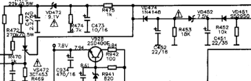
How Regulator with 2 Photocoupler

Working of Regulator with 2 Photocoupler that is :
  • Photocoupler N901 - used as a coupling-off control on the regulator by mikrokontrol. Which is set high and low voltage B + (st-by at the B + voltage is low). Control of the pin-37 POWER mikrokontrol → V610 → VD913 V908 → N901.
  • Photocoupler N903 - used to control on-off the regulator of X-ray circuit protector. X-ray protector circuit of flyback → VD451 → VD452 → SCR VS472. If the flyback voltage regulator over the job will automatically be turned off by N903
  • To disable the X-ray circuit protector, it can be temporarily removed photocoupler N903 first. In normal conditions the voltage at the transistor V474 should be zero.

Regulator Schematics
Trobelshuting there is no voltage for 5v st-by on the secondary :

  1. Disable by removing the first circuit protectors N903
  2. Check the voltage of 300V
  3. Check all transistors
  4. Check the start voltage of 300V by R909 >> R906 to the base of transistor power regulator
  5. Check the feedback C910 >> R904 (to oscillate)
Read More..

Wednesday, October 22, 2014

Build a Car Voltage Regulator Circuit Using LM317

The car cigarette lighter socket does not only light cigarettes, but can be utilized as an electrical channel for powering tools to work on the car such as laptops and other electronic devices. The following circuit diagram shows a way of powering a two-way mobile radio using the LM317T voltage regulator.

The LM317T is an adjustable 3-terminal positive voltage regulator that efficiently provides a load current of 1.5 Amps over an output range of 1.2 V and 37 V. With reference to the circuit, it can accept 14 volts without any hassle and the voltage can be controlled easily with the use of a potentiometer, a 3-terminal resister with sliding contact. The whole circuit will contain the following components:


 Printed Circuit Board (PCB)
Resistor 1 (R1): 270 ohms
Resistor 2 (R2): 2K carbon potentiometer
Capacitor 1 (C1): 100nF
Capacitor 2 (C2): 1uF tantalum
LM317T Voltage Regulator
Heat Sink
DC Power Jacks
Green LED: Power
Red LED: Over Voltage
Zener Diode: over voltage LED switch

The zener diode switches on the over voltage LED if the voltage passing through is larger than the breakdown or preset voltage. The use of zener diode permits a constant amount of voltage and can be very beneficial for devices that inputs the same amount of voltage.

LM317T is cheaply available in the market and is very simple to integrate into several energy system to supply a maximum current or voltage.
Read More..

Ultra Low Drop Linear Regulator

The circuit is a MOSFET based linear voltage regulator with a voltage drop of as low as 60 mV at 1 ampere. Drop of a fewer millivolts is possible with better MOSFETs having lower  RDS(on)  resistance. 

The circuit in Fig.1 uses 15V-0-15V secondary output from a step-down transformer and employs an n-channel MOSFET IRF540 to get the regulated 12V output from DC input, which could be as low as 12.06V. The gate drive voltage required for the MOSFET is generated using a voltage doubler circuit consisting of diodes D1 and D2 and capacitors C1 and C4. To turn the MOSFET fully on, the gate terminal should be around 10V above the source terminal which is connected to the output here. The voltage doubler feeds this voltage to the gate through resistor R1. Adjustable shunt regulator TL431 (IC2) is used here as an error amplifier, and it dynamically adjusts the gate voltage to maintain the regulation at the output.
Ultra Low Drop Linear Regulator Circuit Fig-1 Circuit Fig.1

With adequate heatsink for the MOSFET, the circuit can provide up to 3A output at slightly elevated minimum voltage drop. Trimpot VR1 in the circuit is used for fine adjustment of the output voltage. Combination of capacitor C5 and resistor R2 provides error-amplifier compensation. 

The circuit is provided with a short-circuit crow-bar protection to guard the components against over stress during accidental short at the output. This crow-bar protection will work as follows: Under normal working conditions, the voltage across capacitor C3 will be 6.3V and diode D5 will be in the off state since it will be reverse-biased with the output voltage of 12V. However, during output short-circuit condition, the output will momentarily drop, causing D5 to conduct and the opto-triac MOC3011 (IC1) will get triggered, pulling down the gate voltage to ground, and thus limiting the output current. The circuit will remain latched in this state, and input voltage has to be switched off to reset the circuit. 

Ultra Low Drop Linear Regulator fig-2 Circuit Fig.2

The circuit shown in Fig.2 follows a similar scheme. It can be utilised when the regulator has to work from a DC rail in place of 15V-0-15V AC supply. The gate voltage here is generated using an LM555 charge pump circuit as follows: 

When 555 output is low, capacitor C2 will get charged through diode D1 to the input voltage. In the next half cycle, when the 555 output goes high, capacitor C3 will get charged to almost double the input voltage. The rest of the circuit works in a similar fashion as the circuit of Fig. 1. 

The above circuits will help reduce power-loss by allowing to keep input voltage range to the regulator low during initial design or even in existing circuits. This will keep the output regulated with relatively low input voltage compared to the conventional regulators. 

The minimum voltage drop can be further reduced using low RDS(on) MOSFETs or by paralleling them.


Source by : Ecircuitslab
Read More..

Saturday, October 18, 2014

LM7905 LM7805 Dual Variable Regulator power supply 5 25V

When you want Dual power supply Variable Regulator be simple. I begs for to advise this circuit, because use the integrated circuit LM7805 and LM7905. Make have Voltage +5V to +25V and -5V to -25V unless. Still pay current get about 1A enough with general usability. The important factor is you should use Transformer at enough size doesn’t lower 2A and IC all stick let off the heat with. The detail is other see in circuit picture better sir.
Read More..

Sunday, October 5, 2014

5V Regulator Ultra Low Power Circuit


5V Regulator Ultra Low-Power Circuit by http://www.extremecircuits.net

The accepted cesspool of the regulator is minute compared with that of, say, a 78L05: at an ascribe voltage of 9 V and open-circuit output, it is aloof beneath 50 µA. The ambit consists of a aboveboard bandgap advertence based on T1 and IC1, followed by an amplifier formed by IC2 and T1. The advertence voltage is about 1.22 V, which is aloft by IC2 to 5 V. The achievement voltage can be set to absolutely 5 V with P1. The ascribe voltage may lie amid 6.5 V and 30 V. The best achievement accepted with the present agreement and basic ethics as defined is about 10 mA. For optimum performance, T1a and T1b charge to be identical, which is why a bifold transtor Type MAT02 is used. Other types that may be acclimated are the MAT01, SSM2210 or LM394. In principle, two accepted BC transistors may be used, provided they are called for identical beginning voltage. Circuits IC1 and IC2 are programmable op amps Type OP22. In the case of IC2 this has the account that the aiguille achievement accepted can be set readily by altering the accumulation accepted to the op amp with R9. The akin of the accepted may be amid 500 nA and 400 µA.

Bear in apperception that a beyond achievement accepted requires the use of a added awful rated achievement transistor. Filter R6-C1 prevents any affected pulses extensive the ascribe of IC2. Capacitor C2 improves the adherence of the regulator, decidedly with best beating loading. Note that the ambit has a aerial resistance, so that it is appropriate to abode it in a buried asylum to anticipate causeless alluring and electromagnetic arrest actuality accompanying to the circuit. The regulator was activated with a absolute amount accepted of 1 mA on which was superimposed a square-wave accepted of 10 mA. The analysis after-effects are abbreviated in the table, in which Ig represents the accepted fatigued by the circuit.
Read More..

LM317K 3A Switching Regulator Circuit


LM317K 3A Switching Regulator Circuit

When compared to linear voltage regulators the switching voltage regulators are much power efficient. In the case of linear voltage regulators the difference between the input and output voltage is just wasted and for switching regulators there is almost no such wastage and that’s why the switching regulators have great power efficiency ranging up to 85% . In simple words, the switching regulator operates by taking small bits of energy from the input voltage source and then transferring it to the output with the help of a solid state switch and a control circuitry. Since the switching element is either fully open or closed at any moment, no energy is wasted across it. The control circuit controls the duty cycle of the solid state switch which in turn determines rate at which energy is transferred to the output.

The electronic circuit given here is of a simple and low cost switching regulator using the IC LM317 that can deliver up to 3A of current. The input voltage range of this circuit is between 8 to 35V DC and the output voltage can be adjusted between 1.8 to 32V DC. The output voltage can be adjusted by using the POT R4.
Read More..

Thursday, September 18, 2014

Rotative Speed Regulator Borer Driller Controller

This rotative speed regulator circuit schematic allows to control the holing speed of your borer or driller machine. This project is based on the fact that if the load grows, the voltage decrease and current increase. Use this circuit to control the speed of revolutions of your drilling mill or bench drill.

Driller controller circuit schematic

Circuit Project: Rotative speed regulator borer, driller controller 


Source By : http://www.extremecircuits.net/2012/08/rotative-speed-regulator-borer-driller.html
Read More..

Simple Low Drop 5V Regulator

A 4-cell pack is a convenient, popular battery size. Alkaline manganese batteries are sold in retail stores in packs of four, which usually provide sufficient energy to keep battery replacement frequency at a reasonable level. Generating 5 V from four batteries is, however, a bit tricky. A fresh set of four batteries has a terminal voltage of 6.4 V, but at the end of their life, this voltage is down to 3.2 V. Therefore, the voltage needs to be stepped up or down, depending on the state of the batteries. A flyback topology with a costly, custom designed transformer could be used, but the circuit in the diagram gets around the problem by using a flying capacitor together with a second inductor.

Circuit diagram:

The circuit also isolates the input from the output, allowing the output to go to 0 V during shutdown. The circuit can be divided conceptually into boost and buck sections. Inductor L1 and switch IC1 comprise the boost or step-up section, and inductor L2, diode D1 and capacitor C3 form the buck or step-down section. Capacitor C2 is charged to the input voltage, Vin, and acts as a level shift between the two sections. The switch toggles between ground and Vin+Vout , while the junction of L2, C2 and D1 toggles between –Vin and Vout +Vd1. Efficiency is directly related to the quality of the capacitors and inductors used.

Better quality capacitors are more expensive. Better quality inductors need not cost more, but normally take up more space. The Sanyo capacitors used in the prototype (C1–C3) specify a maximum ESR (effective series resistance) of 0.045 ½ and a maximum ripple current rating of 2.1 A. The inductors used specify a maximum DCR (direct current resistance) of 0.058 ½. Worst-case r.m.s. current through capacitor C2 occurs at minimum input voltage, that is, 400 mA at full load with an input voltage of 3 V. 
Read More..

Friday, September 12, 2014

Simple Low Power Switching Regulator Wiring diagram Schematic

This is the Simple Low Power Switching Regulator Circuit Diagram. A simple battery-powered switching regulator provides 5 V out from a 9-V source with 80% efficiency and 50 mA output capability. When Q1 is on, its collector voltage rises, forcing current through the inductor. The output voltage rises, causing A1`s output to rise. 

Low Power Switching Regulator Circuit Diagram


Simple

Q1 cuts off and the output decays through the load. The 100-pF capacitor ensures clean switching. The cycle repeats when the output drops1ow enough for A1 to turn on Ql. The 1-
Read More..

Tuesday, September 9, 2014

LM2575 and LM2577 Regulator Switching Circuit

Switching regu­lators are available is different schema configurations in­cluding the flyback, feed-forward, push-pull, and non-iso­lated single-ended or single-polarity types. Also, the switching regulators can operate in any of three modes – step-down, step-up, or polarity inverting. rovide the active functions for step-down (back) switching regulator, capable of driving a1A load with excellent line and load regulation. These devices are available in fixed output voltages of 3.3V, 5V, 12V, 15V and an adjustable output version.

LM2575 Regulator Switching Circuit

Requiring a minimum number of external components, these regulators are simple to use and include internal frequency compensation and a fixed-frequency oscillator. LM 2575 series offers a high-efficiency replacement for popular 3-terminal linear regulators. It substantially reduces the size of the heat sink, and in many cases no heat sink is required. Fixed output voltage version is illustrated in figure.
LM2577 Regulator Switching Circuit

The National Semiconductor LM 1577/LM 2577 are monolithic ICs that provide all of the power and control functions for step-up (boost), fly back, and forward converter switching regulators. The device is available in three different output voltage versions: 12 V, 15 V and adjustable.

Via:[http://www.diagramtoday.com/switching-regulators-using-lm-2575-and-lm-2577]
Read More..

Sunday, August 24, 2014

Simple Low Drop 5V Regulator

A 4-cell pack is a convenient, popular battery size. Alkaline manganese batteries are sold in retail stores in packs of four, which usually provide sufficient energy to keep battery replacement frequency at a reasonable level. Generating 5 V from four batteries is, however, a bit tricky. A fresh set of four batteries has a terminal voltage of 6.4 V, but at the end of their life, this voltage is down to 3.2 V. Therefore, the voltage needs to be stepped up or down, depending on the state of the batteries. A flyback topology with a costly, custom designed transformer could be used, but the schema in the diagram gets around the problem by using a flying capacitor together with a second inductor.

Simple Low-Drop 5V Regulator  Circuit diagram:

Simple

The schema also isolates the input from the output, allowing the output to go to 0 V during shutdown. The schema can be divided conceptually into boost and buck sections. Inductor L1 and switch IC1 comprise the boost or step-up section, and inductor L2, diode D1 and capacitor C3 form the buck or step-down section. Capacitor C2 is charged to the input voltage, Vin, and acts as a level shift between the two sections. The switch toggles between ground and Vin+Vout , while the junction of L2, C2 and D1 toggles between –Vin and Vout +Vd1. Efficiency is directly related to the quality of the capacitors and inductors used.

Better quality capacitors are more expensive. Better quality inductors need not cost more, but normally take up more space. The Sanyo capacitors used in the prototype (C1–C3) specify a maximum ESR (effective series resistance) of 0.045 ½ and a maximum ripple current rating of 2.1 A. The inductors used specify a maximum DCR (direct current resistance) of 0.058 ½. Worst-case r.m.s. current through capacitor C2 occurs at minimum input voltage, that is, 400 mA at full load with an input voltage of 3 V. 
Read More..

Friday, August 22, 2014

Remote Controlled Fan Regulator Wiring diagram Schematic

Remote-Controlled Fan Regulator Circuit Diagram. Using this schema, you can change the speed of the fan from your couch or bed. Infrared receiver module TSOP1738 is used to receive the infrared signal transmitted by remote control. The schema is powered by regulated 9V. The AC mains is stepped down by transformer X1 to deliver a secondary output of 12V-0-12V. The transformer output is rectified by full-wave rectifier comprising diodes D1 and D2, filtered by capacitor C9 and regulated by 7809 regulator to provide 9V regulated output. Any button on the remote can be used for controlling the speed of the fan. Pulses from the IR receiver module are applied as a trigger signal to timer NE555 (IC1) via LED1 and resistor R4.


Remote-Controlled
Remote-Controlled Fan Regulator Circuit Diagram

IC1 is wired as a monostable multivibrator to delay the clock given to decade counter-cum-driver IC CD4017 (IC2).Out of the ten outputs of decade counter IC2 (Q0 through Q9), only five (Q0 through Q4) are used to control the fan. Q5 output is not used, while Q6 output is used to reset the counter. Another NE555 timer (IC3) is also wired as a monostable multivibrator. Combination of one of the resistors R5 through R9 and capacitor C5 controls the pulse width.  The output from IC CD4017 (IC2) is applied to resistors R5 through R9. If Q0 is high capacitor C5 is charged through resistor R5, if Q1 is high capacitor C5 is charged through resistor R6, and so on.

Optocoupler MCT2E (IC5) is wired as a zero-crossing detector that supplies trigger pulses to monostable multivibrator IC3 during zero crossing. Opto-isolator MOC3021 (IC4) drives triac BT136. Resistor R13 (47-ohm) and capacitor C7 (0.01µF) combination is used as snubber network for triac1 (BT136). As the width of the pulse decreases, firing angle of the triac increases and speed of the fan also increases. Thus the speed of the fan increases when we press any button on the remote control. Assemble the schema on a general-purpose PCB and house it in a small case such that the infrared sensor can easily receive the signal from the remote transmitter.

Sourced by : Circuitsstream.blogspot.com
Read More..