Wednesday, November 19, 2014
USB FX2 USB 2 0 interface board circuit schematic
There are some things one should be aware of when building the design above:
- Resonator: According to the data sheet, the FX2LP has an on-chip oscillator circuit which requires an external 24MHz (±100ppm) parallel resonant, fundamental mode crystal with 500uW drive level and 12pF (5% tolerance) load capacitors. So, you cant just put any 24MHz crystal there but things dont seem to be as critical as one may expect. Im using a 24MHz fundamental mode crystal (24-MA505 from Reichelt) with 10..15pF caps (or even 32pF).
(Note: In the schematic above, there are 2 crystal oscillators in parallel merely to have both options on the PCB (one of them is an SMD). Only one of them is actually soldered onto the board.) - EEPROM: You can use an optional serial EEPROM to store either USB configuration data or a complete program which is loaded into the microcontrollers RAM at startup. You can leave it away completely to use default USB config data and download firmware via the USB (thereby also changing, the config data, its the so-called ReNumeration thingy). Note, however, that if you leave away the EEPROM, you must still put in both the 2.2k I2C bus pull-up resistors.
- PWR_SEL: For USB-powered operation (500mA max), close a jumper between pins 2 and 3, for externally powered operation, apply 5V and GND to pins 2 and 1, respectively. There is an additional 5V, 3.3V and GND power connector called PWR_HUB to connect with add-on boards.
- For 5V-to-3.3V conversion, you need to use an LDO (low-dropout regulator) like the LM2937. It should have a drop-out of 1.2V max since the USB specs allow the 5V voltage to be as low as 4.5V on the slave side.
- Of course, usual voodoo applies like putting decoupling caps near by and keeping the USB data lines short. A massive ground plane is mandatory, at least for the analog half. Forget about Cypress telling you that you need at least a 4-layer PCB. My regular 2-layer PCB (ground plane on bottom) works stable in high-speed mode even with 3m USB cable.

Thursday, October 23, 2014
0 3 to 1 5V LED Flashlight

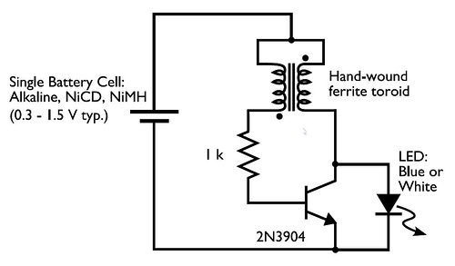


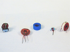
Monday, September 22, 2014
0 50V 2A Bench power supply circuit and description
Circuit diagram
I use the lm10 IC because it has a reference voltage and that’s useful for dc power supply. With two ICs can take different output voltage and amperage. This circuit is protected from short circuit.P2 is for controlling the current at the range of 0-2A. Stabilize the output voltage with R4 on negative pin on op-amp and with R2 & P1 on positive pin.
Op-amp output controls T1 that not let ripple of voltage.T1 increase or decrease ampere of R6 and control the voltage of T5 & T4. Pin 1 is the reference voltage and reference voltage is losing some voltage on R1 that has 100uA . This current passes through P1 too.
Vlose p1=100uA*Rp1
This lose voltage regulate output voltage rate of output current is compare between reference voltage of P3 and lose voltage on R11.T3 is protecting short circuit with R11. For reduce out put voltage to 0v should parallel one resistor 470 ohm in out put. Minimum voltage is 0.4v. The maximum output voltage is fixed with R1b and should not become over of 50v. Therefore your transformer should give 36V, 3A with 4700uF capacitor. T6, T5, T7 need heatsilk.
R1a = 2,2 K
R1b = read the text
R2 = 10 K
R3, R7 = 3.3 k
R4 = 390 Ohm
R5 = 47 K
R6 = 3.3 K 1Watt
R8 = 180 Ohm
R9, R10 = 0.47 Ohm 3Watt
R11 = 0.075 Ohm 2Watt
R12 = 470 Ohm
P1 = 500K liner potentiometer
P2 = 4.7 K potentiometer
P3 = 10 K potentiometer
C1 = 1nF
C2 = 10nF
C3 = 22nF
C4 = 47mF 63v electrolytic
C5 = 4700mF 80v electrolytic
T1, T2 = BC161
T3, T4 = BD141
T5 = BD241
T6, T7 = 2V3055
D1, D2 = 1N4148
D3, D4 = 1N4001
IC1, IC2 = LM10C
author:
e-mail: hamed_iranmehr@yahoo.com
web site: http://www.electronics-lab.com
0 50V 2A Bench power supply circuit and explanation
I use the lm10 IC because it has a reference voltage and that’s useful for dc power supply. With two ICs can take different output voltage and amperage. This circuit is protected from short circuit.P2 is for controlling the current at the range of 0-2A. Stabilize the output voltage with R4 on negative pin on op-amp and with R2 & P1 on positive pin.
Op-amp output controls T1 that not let ripple of voltage.T1 increase or decrease ampere of R6 and control the voltage of T5 & T4. Pin 1 is the reference voltage and reference voltage is losing some voltage on R1 that has 100uA . This current passes through P1 too.
Vlose p1=100uA*Rp1
This lose voltage regulate output voltage rate of output current is compare between reference voltage of P3 and lose voltage on R11.T3 is protecting short circuit with R11. For reduce out put voltage to 0v should parallel one resistor 470 ohm in out put. Minimum voltage is 0.4v. The maximum output voltage is fixed with R1b and should not become over of 50v. Therefore your transformer should give 36V, 3A with 4700uF capacitor. T6, T5, T7 need heatsilk.
R1a = 2,2 K
R1b = read the text
R2 = 10 K
R3, R7 = 3.3 k
R4 = 390 Ohm
R5 = 47 K
R6 = 3.3 K 1Watt
R8 = 180 Ohm
R9, R10 = 0.47 Ohm 3Watt
R11 = 0.075 Ohm 2Watt
R12 = 470 Ohm
P1 = 500K liner potentiometer
P2 = 4.7 K potentiometer
P3 = 10 K potentiometer
C1 = 1nF
C2 = 10nF
C3 = 22nF
C4 = 47mF 63v electrolytic
C5 = 4700mF 80v electrolytic
T1, T2 = BC161
T3, T4 = BD141
T5 = BD241
T6, T7 = 2V3055
D1, D2 = 1N4148
D3, D4 = 1N4001
IC1, IC2 = LM10C
author:
e-mail: hamed_iranmehr@yahoo.com
web site: http://www.electronics-lab.com
