Showing posts with label output. Show all posts
Showing posts with label output. Show all posts
Friday, October 31, 2014
Universal Battery Charger Battery charger for general purpose usage Universal Battery Charger circuit diagram The chargers output voltage is adjust
Universal Battery Charger

Power transistors Q1 and Q2 are connected as series regulators to control the battery chargers output voltage and charge-current rate. An LM-317 adjustable voltage regulator supplies the drive signal to the bases of power transistor Q1 and Q2. Potensiometer R9 sets the output-voltage level. A current sampling resistor, R8 (a 0.1 ohm/5W unit), is connected between the negative output lead and circuit ground. For each amp of charging current that flows through R8, a 100mV output is developed across it. The voltage developed across R8 is fed to one input of comparator U3. The other input of the comparator is connected to variable resistor R10.
As the charging voltage across the battery begins to drop, the current through R8 decrease. Then the voltage feeding pin 5 of U3 decreases, and the comparator output follows, turning Q3 back off, which completes the signals circular path to regulate the batterys charging current.
The charging current can be set by adjusting R10 for the desired current. The circuits output voltage is set by R9

Sunday, August 17, 2014
Simple Subwoofer Amplifier Wiring diagram Schematic with 30W Output power
Simple Subwoofer Amplifier Circuit Diagram with 30W Output power. This schema with 30w output Power schema. This Amplifier schema is very suitable for use in subwoofer amplifier system based on IC SI1030G. Amplifier has 30W output with 8 ohm impedance. Supply voltage required minimum of 12 volts and a maximum of up to 22 volts DC.
Simple Subwoofer Amplifier Circuit Diagram with 30W Output power

Parts List
R1 = 100K
R2 = 1R
C1 = 2.2uF
C2 = 100uF
C3 = 47uF
C4 = 100nF
C5 = 10uF
C6 = 47uF
C7 = 100uF
IC = SI1020GL , SI1030G
Simple Subwoofer Amplifier Circuit Diagram with 30W Output power
Parts List
R1 = 100K
R2 = 1R
C1 = 2.2uF
C2 = 100uF
C3 = 47uF
C4 = 100nF
C5 = 10uF
C6 = 47uF
C7 = 100uF
IC = SI1020GL , SI1030G
Monday, August 11, 2014
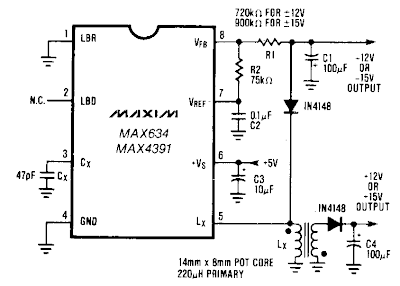
Dual Output dc dc Converter Wiring diagram Schematic
The Dual Output dc-dc Converter Circuit Diagram buck-boost configuration the MAX634 is well suited for dual output dc-dc converters. Only a second winding on the inductor is needed. Typically, this second winding is bifilar-primary and secondary are wound simultaneously using two wires in parallel.
The inductor core is usually a toroid or a pot core. The negative output voltage is fully regulated by the MAX634. The positive voltage is semi-regulated, and will vary slightly with load changes on either the positive or negative outputs.
Dual Output dc-dc Converter Circuit Diagram
Subscribe to:
Posts (Atom)
