Showing posts with label to. Show all posts

Monday, November 17, 2014

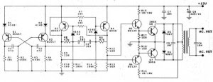
6 to 12 Volt Power Supply Inverter

This inverter circuit can provide up to 800mA of 12V power from a 6V supply. For example, you could run 12V car accessories in a 6V (British?) car. The circuit is simple, about 75% efficient and quite useful. By changing just a few components, you can also modify it for different voltages.


6
Part List:

R1, R4 2.2K 1/4W Resistor
R2, R3 4.7K 1/4W Resistor
R5 1K 1/4W Resistor
R6 1.5K 1/4W Resistor
R7 33K 1/4W Resistor
R8 10K 1/4W Resistor
C1,C2 0.1uF Ceramic Disc Capacitor
C3 470uF 25V Electrolytic Capcitor
D1 1N914 Diode
D2 1N4004 Diode
D3 12V 400mW Zener Diode
Q1, Q2, Q4 BC547 NPN Transistor
Q3 BD679 NPN Transistor
L1 See Notes
MISC Heatsink For Q3, Binding Posts (For Input/Output), Wire, Board
Read More..

Friday, November 14, 2014

How to Build a UPS for USB devices

Portable systems often include circuitry that derives power from an external source, such as USB. When the system disconnects from the USB supply, a battery takes over and supplies current via a dc/dc converter. A diode-OR connection (Figure 1 offers the easiest way to ensure that the supply voltage doesnt sag during this switchover to the battery. The diodes forward voltage drop, however, can reduce battery life and efficiency.

A diode-OR connection is effective but lossy.


 A boost-converter circuit is an improvement over the simple diode-OR connection.

The single-cell, boost-converter circuit with external PFET (Figure 2) is an improvement over the diode-OR connection. The PFET, Q1, coupled with IC1s internal gain block, forms a linear regulator. The USB power supply has a diode-OR connection to Q1s source. Setting the boost converters output to 3.4V allows the drain of Q1 to regulate to 3.3V. This configuration produces negligible loss in Q1. The bus-supply voltage available to USB devices ranges from 4.4 to 5.25V.

When you connect the bus, it forward-biases D1 and causes the boost converter to idle. The converter continues to idle as long as its output remains above the 3.4V regulation point. The bus supply serves the load and activates the current source to charge the battery.


Adjusting R1 allows you to set the current-source output to charge the nickel-metal-hydride cells at a level one-tenth the batterys capacity. Disconnecting the circuit from the USB supply causes the boost converter to cease idling and supply current to the load via the battery. Figure 3 shows that the load current suffers no interruption during a switchover from USB to battery.
Read More..

Thursday, November 13, 2014

ADV7123 Digital to Analog Converter Connection Diagram and Datasheet


This digital-to-analog converter (DAC) integrated circuit is designed for lowest noise performance, both radiated and conducted noise. A recommended connection diagram for the ADV7123 is shown in the following schematic diagram.

According to the ADV7123 datasheet, this device consists of three high speed, 10-bit, video DACs with complementary outputs, a standard TTL input interface, and a high impedance, analog output current source. It used to be applied in digital video systems, image processing, digital radio modulation, color graphics and more.

Additional information on ADV7123 Digital-to-Analog Converter Connection Diagram can be seen in this datasheet of pdf filetype (source: analog.com).

Read More..

Tuesday, November 4, 2014

VGA to TV Converter Circuit

VGA to TV Converter Circuit

This converter circuit basically takes VGA signals and converts it to RGB + composite sync signal which can be fed to TV via SCART connector. VGA card picture components RED, GREEN and BLUE are already at the correct voltage level (0.7Vpp) and has correct impedance (75 ohm) for direct connection to correspondign inputs in the TV.
VGA to TV Converter Ciruit


VGA to TV Converter Printed Circuit Board (PCB)


For combining separate horizonal and vertical sync signal from VGA card to one composite sync signal needs a sync signal conversion which is feed to TV video in pin in SCART connector. The tv converter circuit has also sends correct level signal to the TV RGB input enabling control pin in the SCART connector (pin 16).
The circuit is simply based on one TTL chip with four XOR ports, two resistors and two capacitors. TTL chip was logical choise because VGA sync signals are TTL level signals.

The sync signal combiner has a system to adjust to different sync polarities so that it always makes correct composite sync signals. VGA card uses different sync signal polarities to tell the monitor which resolution is used. This circuit adjusts to sync signal polarity changes in less than 200 milliseconds, which is faster than setting time of a normal VGA monitor in the display mode change. The tv converter circuit needs well regulates +5V (+/-5%) power supply and takes about 120 mA current.

VGA to TV converter parts list are as follow:

Main circuit

U1 74LS86 (74HC86 or 74HCT86 can also be used)

C1 22 microfarads 16V electrolytic capacitor

C2 use 47 uF 16V electrolytic for more reliable operation (22 uF listed schematic can cause problems in some cases)

R1,R2 2.2 kohm, 1/4 W

R3,R4,R5 2.2 kohm, 1/4 W

R6,R7,R9 47 ohm, 1/2 W

R8 120 ohm, 1/2 W

T1,T2 BC547B (2N2222 should also work but note the different pinout)

P1 15 pin SUB-D connector (DE-15)

Output connector

21 pin EURO/SCART connector

Wiring:

Red, Green, Blue and Composite Sync lines should be wired using 75 ohm coaxial cable for best picture quality, but can be replaced with normal shielded wire.

Power supply components

7805 regulator chip

100 uF electrolytic 25V

10 uF electrolytic 16V

100 nF polyester or ceramic condensator

Wall adapter which outputs 8-18V DC and 150 mA or more current

Connector for connecting wall adaptor to circuit 
Read More..

Monday, November 3, 2014

Cheap 12V to 220V Inverter

Even though today’s electrical appliances are increasingly often self-powered, especially the portable ones you carry around when camping or holidaying in summer, you do still sometimes need a source of 230 V AC - and while we’re about it, why not at a frequency close to that of the mains? As long as the power required from such a source remains relatively low - here we’ve chosen 30 VA - it’s very easy to build an inverter with simple, cheap components that many electronics hobbyists may even already have.

Though it is possible to build a more powerful circuit, the complexity caused by the very heavy currents to be handled on the low-voltage side leads to circuits that would be out of place in this summer issue. Let’s not forget, for example, that just to get a meager 1 amp at 230 VAC, the battery primary side would have to handle more than 20 ADC!. The circuit diagram of our project is easy to follow. A classic 555 timer chip, identified as IC1, is configured as an astable multivibrator at a frequency close to 100 Hz, which can be adjusted accurately by means of potentiometer P1.

Cheap 12V to 220V Inverter Circuit diagram:

Inverter

As the mark/space ratio (duty factor) of the 555 output is a long way from being 1:1 (50%), it is used to drive a D-type flip-flop produced using a CMOS type 4013 IC. This produces perfect complementary square-wave signals (i.e. in antiphase) on its Q and Q outputs suitable for driving the output power transistors. As the output current available from the CMOS 4013 is very small, Darlington power transistors are used to arrive at the necessary output current. We have chosen MJ3001s from the now defunct Motorola (only as a semi-conductor manufacturer, of course!) which are cheap and readily available, but any equivalent power Darlington could be used.

These drive a 230 V to 2 × 9 V center-tapped transformer used ‘backwards’ to produce the 230 V output. The presence of the 230 VAC voltage is indicated by a neon light, while a VDR (voltage dependent resistor) type S10K250 or S07K250 clips off the spikes and surges that may appear at the transistor switching points. The output signal this circuit produces is approximately a square wave; only approximately, since it is somewhat distorted by passing through the transformer. Fortunately, it is suitable for the majority of electrical devices it is capable of supplying, whether they be light bulbs, small motors, or power supplies for electronic devices.

PCB layout:
invertor-circuit-diagram


Parts List :
Resistors
R1 = 18k?
R2 = 3k3
R3 = 1k
R4,R5 = 1k?5
R6 = VDR S10K250 (or S07K250)
P1 = 100 k potentiometer
Capacitors
C1 = 330nF
C2 = 1000 µF 25V
Semiconductor
T1,T2 = MJ3001
IC1 = 555
IC2 = 4013
Miscellaneous
LA1 = neon light 230 V
F1 = fuse, 5A
TR1 = mains transformer, 2x9V 40VA (see text)
4 solder pins

Note that, even though the circuit is intended and designed for powering by a car battery, i.e. from 12 V, the transformer is specified with a 9 V primary. But at full power you need to allow for a voltage drop of around 3 V between the collector and emitter of the power transistors. This relatively high saturation voltage is in fact a ‘shortcoming’ common to all devices in Darlington configuration, which actually consists of two transistors in one case. We’re suggesting a PCB design to make it easy to construct this project; as the component overlay shows, the PCB only carries the low-power, low-voltage components.

The Darlington transistors should be fitted onto a finned anodized aluminum heat-sink using the standard insulating accessories of mica washers and shouldered washers, as their collectors are connected to the metal cans and would otherwise be short-circuited. An output power of 30 VA implies a current consumption of the order of 3 A from the 12 V battery at the ‘primary side’. So the wires connecting the collectors of the MJ3001s [1] T1 and T2 to the transformer primary, the emitters of T1 and T2 to the battery negative terminal, and the battery positive terminal to the transformer primary will need to have a minimum cross-sectional area of 2 mm2 so as to minimize voltage drop.

The transformer can be any 230 V to 2 × 9 V type, with an E/I iron core or toroidal, rated at around 40 VA. Properly constructed on the board shown here, the circuit should work at once, the only adjustment being to set the output to a frequency of 50 Hz with P1. You should keep in minds that the frequency stability of the 555 is fairly poor by today’s standards, so you shouldn’t rely on it to drive your radio-alarm correctly – but is such a device very useful or indeed desirable to have on holiday anyway? Watch out too for the fact that the output voltage of this inverter is just as dangerous as the mains from your domestic power sockets.

So you need to apply just the same safety rules! Also, the project should be enclosed in a sturdy ABS or diecast so no parts can be touched while in operation. The circuit should not be too difficult to adapt to other mains voltages or frequencies, for example 110 V, 115 V or 127 V, 60 Hz. The AC voltage requires a transformer with a different primary voltage (which here becomes the secondary), and the frequency, some adjusting of P1 and possibly minor changes to the values of timing components R1 and C1 on the 555.


Read More..

Thursday, October 23, 2014

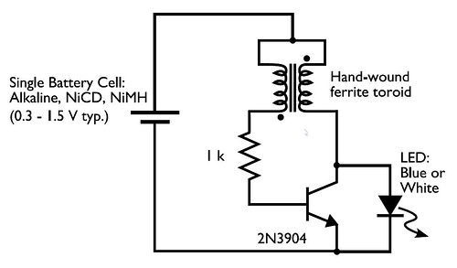
0 3 to 1 5V LED Flashlight

Circuit Project: 0.3 to 1.5V LED Flashlight

Its a little wisp of a circuit that allows you to drive a blue or white LED from a low voltage. Normally, if you want to light up a blue or white LED you need to provide it with 3 - 3.5 V, like from a 3 V lithium coin cell. But a 1.5 V battery like a AA cell simply will not work. But using the Joule Thief, it works like a charm. Not only does it work with a brand new battery, but it works until the battery is nearly dead-- down to 0.3 V. Thats well below the point where your other toys will tell you the battery is dead, so it can steal every last joule of energy from the battery (hence the name). To learn how to make one, watch the video, which is available in a variety of formats.

Circuit Project: 0.3 to 1.5V LED Flashlight

Circuit Project: 0.3 to 1.5V LED Flashlight


Circuit Project: 0.3 to 1.5V LED Flashlight


Circuit Project: 0.3 to 1.5V LED Flashlight
Read More..

6 to 15 Volt DC Converter

A very efficient 6V to 15V DC to DC converter using LM2585 is publicized at this time. LM2585 is a monolithic integrated voltage converter IC with the intention of can be situated used stylish various applications like flyback converters, boost converters, advance converters, multiple output converters and the rest. The circuit requires lowest possible amount of outdoor components and the IC can source up to 3A output current.
at this juncture the IC is wired for instance a boost converter somewhere resistors R1 and R2 are used to established the output voltage .The junction of R1 and R2 is connected to the comment pin of IC1. Capacitor C4 is the input filter while capacitor C1 the filter on behalf of output. set of contacts comprising of resistor R1 and capacitor C2 is intended for frequency compensation. Inductor L1 provisions the energy for acquiring boost conversion.


6 to 15 Volt DC Converter

Read More..

Monday, October 20, 2014

New 100W Inverter 12VDC to 220VAC circuit diagram

The following diagram is an inverter circuit which will give you 220V AC 50Hz with maximum power of 100W. This inverter built using transistors both the square wave generator and the amplifier.The Q1 and Q2 used generate square wave. Q5-Q8 amplify the signal and the transformer to increase the AC/square wave current from 12VAC to 220V AC 50HZ.

100W Inverter 12VDC to 220VAC circuit diagram

100W Inverter 12VDC to 220VAC circuit diagram


Inverter PCB layout


Read More..

Build a 12V To 24V DC DC Converter Circuit Diagram

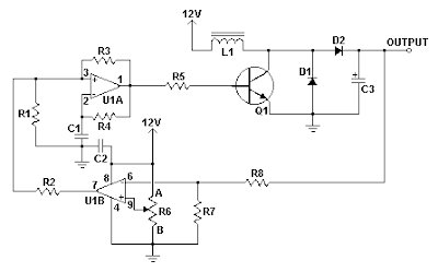
Build a 12V To 24V DC-DC Converter Circuit Diagram.This simple 12V To 24V DC-DC Converter Circuit Diagram can provide up to 24V from a 12V source. It can be used to run radios, small lights, relays, horns and other 24V accessories from a 12V vehicle with a maximum draw of about 800mA. 

It can be used to charge one 12V battery from another, or step up the voltage just enough to provide necessary overhead for a 12V linear regulator. Using one op-amp as a square wave oscillator to ring an inductor and another op-amp in a feedback loop, it wont drift around under varying loads, providing a stable 24V source for many applications. With a wide adjustment in output this circuit has many uses.

 12V To 24V DC-DC Converter Circuit Diagram

12V To 24V DC-DC Converter Circuit Diagram

Parts

Part
Total Qty.
Description
Substitutions
R1, R2, R3, R4, R8, R76100K 1/4W Resistor
R51470 Ohm 1/2W Resistor
R6110K Linear Pot
C110.01uF Mylar Capacitor
C210.1uF Ceramic Disc Capacitor
C31470uF 63V Electrolytic Capacitor
D111N4004 Rectifier Diode
D21BY229-400 Fast Recovery DiodeSee Notes
Q11BC337 NPN Power Transistor
U11LM358 Dual Op Amp IC
L11See Notes
MISC1Board, Wire, Socket For U1, Case, Knob For R6, Heatsink for Q1

Notes

  • R6 sets the output voltage. This can be calculated by Vout = 12 x (R8/(R8+R7)) x (R6B/R6A).
  • L1 is made by winding 60 turns of 0.63MM magnet wire on a toroidial core measuring 15MM (OD) by 8MM (ID) by 6MM (H).
  • D2 can be any fast recovery diode rated at greater then 100V at 5A. It is very important that the diode be fast recovery and not a standard rectifier.
  • Q1 will need a heatsink.


Sourced By Circuitsstream
Read More..

Simle DC to AC Inverter by IC 555

This be basic AC inverter Circuit. Convenient for the initiator who have to is extremely fond of something experience. Because of use IC 555 highly popular, perform produce the frequency ,then enlarge with transistor NPN and PNP number TIP41 and TIP42 drive the coil transformer. Get by can pay Voltage output about 120V to 230V at frequency 50Hz. By have R4 perform control the frequency and should use. Voltage supply about 5V to 15V the detail sees in circuit picture sir. Link


Read More..

Friday, October 17, 2014

Build a100W Inverter 12V to 220V Circuit Diagram

How to Build a100W Inverter 12V to 220V Circuit Diagram. When use the electric appliances that want 220V AC 50HZ, which have small-sized about 100Watt not exceed. By when you apply outside home, as a result have to have Mini power inverter about 100Watt, perform modify from work electricity forces of battery 12V give tall fair the work. 

100W Inverter 12V to 220V Circuit Diagram
 
100W
 If you are New user electronics or want to economize or want to build electronics project use by oneself. I begs for to advise this circuit , because it uses , transistor number BC557 or the number replaces, perform oscillator generator. Then have power transistor 2N3055 numbers perform to drive coil transformer for converter voltage give tall go up 220V AC 50HZ at the electric power about 100 watt not exceed. When apply to transformer about 2A-3A. Picture circuit detail and like model PCB Board.

 PCB


Read More..

Thursday, October 16, 2014

How to Lights Control for Model Cars

The author gave his partner a radio controlled (RC) model car as a gif t. She found it a lot of fun, but thought that adding realistic lights would be a definite improvement. So the author went back to his shed, plugged in his soldering iron, and set to work equipping the car with realistic indicators, headlights, tail lights and brake lights.

Lights Control for Model Cars Circuit Diagram

The basic idea was to tap into the signal from the radio control receiver and, with a bit of help from a microcontroller, simulate indicators using flashing yellow LEDs and brake lights using red LEDs. Further red LEDs are used for the tail lights, and white LEDs for the headlights. Connectors JP4 and JP5 (channel 0) are wired in parallel, as are JP6 and JP7 (channel 1), allowing the circuit to be inserted into the servo control cables for the steering and drive motor respectively. The ATtiny45 micro-controller takes power from the radio receiver via diode D1. T1 and T2 buffer the servo signals to protect IC1’s inputs from damage. 
IC1 analyses the PWM servo signals and gen-erates suitable outputs to switch the LEDs via the driver transistors. T3 drives the two left indicators (yellow), T4 the two right indica-tors, and T5 the brake LEDs (red). The red tail lights (JP2-8 and JP2-8) and the white head-lights (JP2-9 and JP2-10) are lit continuously. The brake lights are driven with a full 20 mA, so that they are noticeably brighter than the tail lights, which only receive 5 mA. If you wish to combine the functions of tail light and brake light, saving t wo red LEDs, sim-ply connect pin 10 of JP2 to pin 14 and pin 12 to pin 16. Then connect the two combined brake/tail LEDs either at JP2-5 and JP2-6 or at JP2-7 and JP2-8.

JP3 is provided to allow the use of a separate lighting supply. This can either be connected to an additional four-cell battery pack or to the main supply for the drive motor. The val-ues given for resistors R8 to R17 are suitable for use with a 4.8 V supply. JP2 can take the form of a 2x10 header.

As usual the sof t ware is available as a free download from the Elektor web pages accom-panying this article[1], and ready-programmed microcontrollers are also available. The microcontroller must be taught what servo signals correspond to left and right turns, and to full throttle and full braking. First connect the fin-ished circuit to the radio control electronics in the car, making sure everything is switched of f. Fit jumper JP1 to enable configuration mode, switch on the radio control transmit-ter, set all proportional controls to their cen-tre positions, and then switch on the receiver. The indicator LEDs should first flash on both sides. Then the car will indicate left for 3 s: during this time quickly turn the steering on the radio control transmitter fully to the left and the throt tle to full reverse (maximum braking).

Hold the controls in this position until the car starts to indicate right. Then set the controls to their opposite extremes and hold them there until both sides flash again. Now, if the car has an internal combustion engine (and so cannot go in reverse), keep the throttle control on full; if the car has an electric motor, set the throttle to full reverse. Hold this position while both sides are flashing.  
Read More..

Sunday, October 5, 2014

2N3055 DC 12V to DC 6V 7 5V 9V Converter


This circuit is DC to DC converter model step down voltage. That can modify voltage input 12V DC from be DC 6V , 7.5V and 9V by have the size current about 1A – 2 Amp think. Be easy circuit use Zener diode maintain one’s position voltage. Be stable and have transistor 2N3055. 
Read More..

Friday, September 26, 2014

How to Design and Make Transformer at Home

Almost every electronic circuit needs a separate power supply, which may be a battery or a rectified power supply. Here we will deal with the design and making  of small transformers that are normally used in conjunction with mains-operated power supplies.
This will help electronic hobbyists to design and construct their own transformers according to their needs. In the following pages, a simplified design procedure is given so as to obtain satisfactorily designed transformers. However, the design procedure is often a matter of trial and error.

The tables provided here cut calculations short and help the designer to choose the proper size of wire or core lamination. Only relevant data and calculations are provided so that the designer is not confused by unnecessary details.

The transformer

A transformer has two or more windings of insulated copper wire over an iron core. They are: one primary winding and one or more secondary windings. Each winding is electrically isolated from the other, but they are magnetically coupled with the help of a laminated iron core. Small transforrners have a shell type construction, i.e. the windings are surrounded by the core as shown in Fig. 1. The power delivered by the secondary is actually transferred from the primary, but at a voltage level determined by the turns ratio of the two windings.

Making the Preliminary Transformer design

As the first step to the design of a transformer, the primary and secondary voltage ratings and the secondary current rating must be clearly stated. Then decide on the core material to be used: ordinary steel stampings or cold rolled grain oriented (CRGO) stampings. CRGO has a higher allowable flux density and lower losses.

Core area = 1.l52 x root of (Output voltage x output current) sq. cm.

For transformers with multiple secondaries, the sum of the output volt-amp. product of each winding is to be used. The number of tums on the primary and secondary windings is decided by the turns per volt ratio as:

Turns per volt = 1/ (4.44 X l0^-4 frequency x core area x flux density)

Here, the frequency is 50Hz for Indian domestic mains supply. The flux density can be taken as about 1.0 Weber/ sq. m. for ordinary steel stampings and about 1.3 Weber/ sq. m. for CRGO stampings.

Primary winding design

The current in the primary winding is given by:

Primary Current = Sum of (output volts x output amps)/(Primary volts x efficiency)

The efficiency of small transformers varies between 0.8 to 0.96. A value of 0.87 can be used for ordinary transformers. The proper wire size has to be selected for the winding. The wire diameter depends on the current to be supplied by the winding and the allowable current density of the wire. The current density may be as high as 233 amps/ sq. cm. in small transformers and as low as 155 amps/sq. cm. in large ones. Usually, a value of 200 amps/ sq. cm. can be taken, on whose basis Table 1 is given.

The number of tums in the primary winding is given by:

Primary turns = Turns per volt x primary volts.

The space taken up by the winding will depend on the insulation thickness, method of winding and the wire diameter. Table I gives the approximate values of the turns per square cm. from which we can estimate the window area occupied by the primary winding.

Primary Winding Area = Primary turns/Turns per sq. cm. from Table1

Secondary winding design

Since we have assumed that we know the secondary current rating, we can find out the wire size for the secondary winding by referring to Table 1 directly.

The number of turns on the secondary is calculated in the same way as for the primary, but about 3% extra turns are to be added to compensate for the internal drop of secondary voltage of the transformer, upon loading. Thus,

Secondary Turns = 1.03 (turns per volt x secondary volts)

The window area required for secondary winding is found from Table1 as

Secondary window area = Secondary Turns/Turns per sq. cm from Table1


Core size

The main criterion in selecting the core is the total window area of winding space available.

Total window area = Primary window area + sum of secondary window areas + space for former and insulation

Some extra area is required to accommodate the former and insulation between windings. The actual amount of extra area varies, although 30% may be taken to start with but may have to be modified later. The suitable core sizes having a larger window area are selected from Table ll. . Taking into account the gap between laminations while stacking them (the core stacking factor taken as 0.9), we have

Gross core area = Core Area/0.9 sq.cm.

ln general, a square central limb is preferred. For this, the width of the tongue of lamination is

Tongue width = root of Gross core area cm.

Now refer to Table ll again and finally select the proper i core size, with sufficient window area and a close value of the tongue width as calculated. Adjust the stack height as required to obtain the required core section.

Stack height = Gros core area/Actual tongue width cm.

The stack should not be much less than the tongue width but may be more. However, it should not be more than 1% times the tongue width.


How to Design and Make a Transformer finally

The windings are wound on an insulating former which .fits over the center limb of the core.The primary is usually wound first, then the secondary, with insulation between windings, A final insulating layer is provided over the windings to protect them from mechanical damage. When thin wires are used, their ends must be soldered to thicker wires for bringing the terminals outside the former. The laminations are assembled over the former with alternate laminations reversed in assembly. The laminations must be held together tightly by a suitable clamping frame or by screws (if holes are provided in the laminations).


Shield

lt is a good practice to use an electrostatic shield between the primary and secondary windings to prevent disturbances from passing through to the secondary from the primary. The shield is made out of a copper foil which is wound between the two windings for slightly over a tum. Insulation must be provided along the length of the foil and care taken so that the- two ends of the foil do not touch each other. A wire soldered to the foil is bought out and connected to the ground.


A practical design example can be witnessed below:


Read More..

Monday, September 22, 2014

500W low cost 12V to 220V inverter circuit and explanation

Using this circuit you can convert the 12V dc in to the 220V Ac. In this circuit 4047 is use to generate the square wave of 50hz and amplify the current and then amplify the voltage by using the step transformer.


author: Ashad Mustufa
e-mail: mustufa66@hotmail.com
web site: http://www.electronics-lab.com

Circuit diagram

How to calculate transformer rating
The basic formula is P=VI and between input output of the transformer we have Power input = Power output
For example if we want a 220W output at 220V then we need 1A at the output. Then at the input we must have at least 18.3V at 12V because: 12V*18.3 = 220v*1
So you have to wind the step up transformer 12v to 220v but input winding must be capable to bear 20A.


Read More..

Thursday, September 18, 2014

Mobile phone Circuits to Get Even smaller

Transceivers, appliances such as mobile phones that can send and receive messages, have become smaller and smaller over the last few years, but users are about to experience a new meaning in miniaturisation. 

Research at The Hong Kong University of Science & Technology (HKUST) has successfully combined a unique system architecture and new circuit design techniques to reduce them in size like never before. 
Principal Investigator Dr Howard Luong said the handset of a typical mobile phone today may contain between 150 and 300 separate electrical components.
His research group proposed and demonstrated circuit techniques that make it possible to combine many of these components to a single chip and therefore to significantly reduce the size of circuitry (see example in graphic). A US patent has been granted for one of the circuit techniques. 
 
The transformation applies to the CMOS (Complimentary Metal-Oxide Semiconductor) manufacturing process, which can produce integrated circuits and systems with the highest integration level at the lowest cost. Applying new techniques to the CMOS process, Dr Luongs research enables many “off-chip components to be combined to realize a system-on-chip. But, he said, “this integration created great challenges in circuit implementation.” Part of the research was to solve the problems by new circuit design techniques.
 
The system architecture and circuitry go hand in hand, he added. “They must both work, or neither will be useful.
The resulting design gives the highest component integration in the smallest chip area ever reported, said Dr Luong.
In his design, all off-chip components are fitted into a central chip measuring 36 mm with packaging, and 8mm without being packaged.
Dr Luong’s miniaturisation method means appliances will soon be made for even lower cost and lower power consumption in addition to being much smaller in size and lighter in weight.
With the lowering of cost, size and power, many new and interesting applications will become possible and practical,” he said.
Low-power wireless transceivers, for example, could be integrated into implanted devices such as heart pacemakers to wirelessly transmit and receive information between patients and doctors or monitoring systems.
Wearable mobile phones as small as wrist watches at an affordable price could also become a reality.

Auther
Principal Investigator
Dr Howard Luong
Read More..

Wednesday, September 10, 2014

4 5V To 12V DC


This ic 4.5V to 12V boost schema.You all can get lots of advantages through this schema.Here I have used famous IC LM2698.


Note

# input supply voltage range is 2.2V to 17V DC and outputs ranging from 2.2V to 17V DC

# IC can deliver only up to 400mA.So dont connect lodes more than that

# Build this schema on a PCB
Read More..

Saturday, September 6, 2014

How to Build a 2 to 4 Wire Audio Converter

This audio converter schema maintains 40 dB of isolation between the two halves of entry and exit of a four-line son, while allowing a line connecting two son. A balancing potentiometer, R, adjusts the gain of zero lC2to crossing the inlet to the outlet .

The adjustment is done in terms of work just after installation by inserting a 1 kHz tone at the entrance of four son and setting R to the minimum output signal 82-ohm dummy-load resistor is placed between two wire terminals .

 2 to 4 Wire Audio Converter Circuit Diagram

How

Read More..

Wednesday, September 3, 2014

230 Volt AC To Inverter Switching Wiring diagram Schematic


Description

                  Before three weeks i am introduced  inverter schema diagram but the schema not included ac to inverter switching part so today i introducing a 230 Volt Ac to inverer switching schema diagram .

Circuit showing a inverter switching  . Here i have used  bc 558 ,BC 548 and a relay for making this schema . 230 volt connected to the base of the transistor Q1.When the power is ON positive volt coming to the base of the transistor so the relay schema is open and load working in 230 V AC .When the power is OFF ground voltage coming to the base of the transistor so the Base of the Q2 is positive there for the   relay schema closed and load working in inverter input .Part list and applications are showing below. 

Part List

Component No: Value  Usage
R1 100KΩ Emitter Load
R2 10K Ω Base Biasing 
R3180KΩ  Current Limiting 
Q1BC558  Switching  
Q2BC548   Switching 
D1 IN4007   Relay Balancing 
RL112 V  Inverter Switching 
Read More..

Monday, September 1, 2014

230 Volt AC To Inverter Switching Wiring diagram Schematic

230

Description
Before three weeks i am introduced  inverter schema diagram but the schema not included ac to inverter switching part so today i introducing a 230 Volt Ac to inverer switching schema diagram .
Circuit showing a inverter switching  . Here i have used  bc 558 ,BC 548 and a relay for making this schema . 230 volt connected to the base of the transistor Q1.When the power is ON positive volt coming to the base of the transistor so the relay schema is open and load working in 230 V AC .When the power is OFF ground voltage coming to the base of the transistor so the Base of the Q2 is positive there for the relay schema closed and load working in inverter input .Part list and applications are showing below. Link

Part List

Component No: Value  Usage
R1 100KΩ Emitter Load
R2 10K Ω Base Biasing 
R3180KΩ  Current Limiting 
Q1BC558  Switching  
Q2BC548   Switching 
D1 IN4007   Relay Balancing 
RL112 V  Inverter Switching 
Read More..