Showing posts with label supply. Show all posts

Tuesday, November 18, 2014

Power Supply Variable 1 3V 12 2V 1A Circuit

Power supply circuit to generate output below were variations between 1.3V DC to 12.2V DC with 1A current. In addition, the power supply circuit is also equipped with over-current protection or shield against belebih flow. Power supply circuit is very simple, but the quality is quite good, made her basiskan regulator IC LM723 is a pretty legendary.


1.3V

Description:

R2 to set the output voltage. The maximum current is determined by R3, over-current protection circuit inside the LM723 to detect the voltage on R3, if it reaches 0.65 V, the voltage output will be off her. So the current through R3 can not exceed 0.65 / R3 although output short-circuit in his.

C3 and C4 are ceramic capacitors, as much as possible directly soldered to the PCB, this is because the LM723 is prone to oscillation that is not cool.

LM723 works with 9.5V input voltage to 40 V DC and the LM723 can generate its own current of 150mA when the output voltage is not more than 6-7V under input voltage.

Specifications:

Output (value estimated):

Vmin = (R4 + R5) / (R5 * 1.3)
Vmax = (7.15 / R5) * (R4 + R5)
Imax = 0.65/R3
Max. Power on R3: 0.42/R3
Min. DC Input Voltage (pin 12 to pin 7): Vmax + 5

Component List:

B1 40V/2.5A
C1 2200uF (3300uF even better)
C2 4.7uF
C3 100nF
C4 1NF
C5 330nF
C6 100uF
Green LED D1
D2 1N4003
F1 0.2A F
F2 2A M
IC1 LM723 (in a DIL14 plastic package)
R1 1k
R2 Pot. 5k
R3 0.56R/2W
R4 3.3k
R5 4.7k
S1 250V/1A
T1 2N3055 on a heatsink 5K / W
TR1 220V/17V/1.5
Read More..

Power supply with Z2C

Power supply with Z2C tubes are designed specifically to provide power supply voltage to the EL-34 tube amplifier push-pull in the previous article. Power supply with Z2C tube to tube power amplifier is made with a tube rectifier Z2C. Just as the power supply for power amplifier tube earlier, power supply also uses a filter 3 levels with kapsitor electrolyte. Circuit power supply with tube rectifier Z2C can give +210 VDC output voltage. A complete range of power supply for power amplifier tube can be seen in thethe following figure .

Power


Z2C on the rectifier tube in power supply with tube above require a supply voltage for the filaments taken from the other side of the transformer secondary. Power supply with Z2C tube is a power supply that dapt used as a substitute power supply for power amplifier tubes with a diode in previous articles.
Read More..

Monday, November 17, 2014

6 to 12 Volt Power Supply Inverter

This inverter circuit can provide up to 800mA of 12V power from a 6V supply. For example, you could run 12V car accessories in a 6V (British?) car. The circuit is simple, about 75% efficient and quite useful. By changing just a few components, you can also modify it for different voltages.


6
Part List:

R1, R4 2.2K 1/4W Resistor
R2, R3 4.7K 1/4W Resistor
R5 1K 1/4W Resistor
R6 1.5K 1/4W Resistor
R7 33K 1/4W Resistor
R8 10K 1/4W Resistor
C1,C2 0.1uF Ceramic Disc Capacitor
C3 470uF 25V Electrolytic Capcitor
D1 1N914 Diode
D2 1N4004 Diode
D3 12V 400mW Zener Diode
Q1, Q2, Q4 BC547 NPN Transistor
Q3 BD679 NPN Transistor
L1 See Notes
MISC Heatsink For Q3, Binding Posts (For Input/Output), Wire, Board
Read More..

Power supply with driver TEA1507

Power supply with driver TEA1507 is mostly used by TV branded PHILIPS. Power Supply has an efficiency rate of up to 90% - thus requiring less cooling, as well as stand-by power required is less than 1 watt.

Power Supply with TEA driver is equipped with a variety of surge protector that has a high reliability - not easily damaged if any part of a damaged power supply circuit and power transistor or FET heat is not easily damaged. Power supply circuits are dapatapat working on ac input voltage between 85 up to 275v. The way it works with the driver circuit power supply TEA 1507 is quite simple, so easy tracking of damage to the circuit.


The picture above is the basic power supply circuit with TEA1507
Read More..

Thursday, November 13, 2014

single supply NE5532 preamplifier circuit

By the peoples suggestion I bought myself a breadboard and decided to implement simple (I would even say trivial) single-supply NE5532 chip preamp. Lets see what was done.

Single-supply NE5532 chip preamp made on the breadboard

Single-supply preamp schematic
I dropped PSU filters and Zenner diode voltage limiter, since used lab PSU with 15 V voltage.
Amplifying resistors are selected to be the same (and thus preamp actually becomes a real one with amplifying ratio equal to 2) and to be equal to the input chain resistance (single supply shift made as resistor-based voltage divider and input resistor) to minimize bias current. Thats why there are so many resistors on the actual scheme to match resistance.
Now the results.

Square wave signal
Square wave signal has noticeble peaks at the edges, lets see them in details

Square wave signal peak details
Given the huge amplitude of the input signal (more than a volt) this may be not a limiting factor actually.
What is a real problem, is the input signal range as a whole. Since I used 15V as a supply voltage, its inner ground will be roughly at 7.5 V (there is an appropriate voltage divider attached to the non-inverting input signal), so having total output amplitude of 4 V may be not appropriate for the chip operational amplifier.

Big sine signal cut
Experiments showed that this chip preamp operates correctly when resulted output signal does not exceed 1/10 of the supply voltage (i.e. about 1.2 V max). Triangle and sine signals after some level (when input signal amplitude is about 3-4 V) start producing reversed output signal in the cut area above, i.e. in the middle of the cut line small sine or triangle signal starts growing.
Now question, why do we need chip preamp for the chip amplifier? I believe that the main reason for preamp is to allow to connect power amplifier which may have not very high input resistance, so small preamp with good characteristics (like huge input resistance and very small output one) will not distort small enough input signal. But I think that most of the modern chip sound amplifiers like LM3886 already have big enough input resistance (as all others they have differential amplifier as the first cascade), maybe not that high if would be built with field-effect transistors, but I wonder if that is ever noticeble.
http://www.ioremap.net/node/141
Read More..

Friday, November 7, 2014

LM317 variable power supply

A truly timeless circuit. LM317 is a versatile and highly efficient 1.2-37V voltage regulator that can provide up to 1.5A of current with a large heat sink. Its ideal for just about any application. This was my first workbench power supply and I still use it.

 LM317 variable power supply Circuit Diagram


 lm317 variable power supply circuit diagram

Since LM317 is protected against short-circuit, no fuse is necessary. Thanks to automatic thermal shutdown, it will turn off if heating excessively. All in all, a very powerful (and affordable!) package, indeed.

Although LM317 is capable of delivering up to 37V, the circuit pictured here is limited to 25V for the sake of safety and simplicity. Any higher output voltage would require additional components and a larger heat sink.

Make sure that the input voltage is at least a couple of Volts higher than the desired output. Its ok to use a trimmer if youre building a fixed-voltage supply.Problems:Follow all the safety precautions when working with mains voltage. Insulate all connections on the transformer.

Possible uses:Variable workbench power supply, fixed-voltage supply... Just about any possible application when no more than 1.5A is necessary.
Read More..

Sunday, November 2, 2014

100 watt Hiwatt amplifier model DR 103 power supply schematic circuit diagram

Description :
100 watt Hiwatt amplifier model DR 103 power supply schematic circuit diagram
Read More..

Tuesday, October 28, 2014

Minimal low supply rail detection

At this point’s a minimal low supply rail detection circuit with the purpose of expenditure peanuts and takes a short time ago 20 minutes or else so to become. Its power consumption is quite low, so it may perhaps definitely survive built into battery-powered campaign. as an alternative of using an op amp, the circuit is built around three low-cost transistors (Q1-Q3). Diodes D1-D3 form a 1.8V voltage reference (Vref) used for the emitter of Q1. If the voltage across the voltage wall formed by R1 and VR1 is a reduced amount of than this, Q1 turns on and food Q2 with foundation bias current.

Rail

This turns on Q3 here proportion to this bias current which subsequently drives LED1. The brightness of the LED gives an indication of the severity of the low voltage condition. The brighter the LED, the minor the supply voltage. Trimpot VR1 is adjusted so to facilitate LED1 really comes on by the desired low-voltage promontory. The current consumption is typically take away than 2mA at what time LED1 is rotten. in conclusion, the price exposed in support of RLED is right for 6-12V surgery. For other voltages, RLED can ensue calculated using the formula RLED = (Vcc - 1.8)/0.01 (this equates to a current of with reference to 10mA).
Read More..

Thursday, October 23, 2014

12V 3A Power Supply Circuit Diagram

This circuit provides a 12V regu-lated power supply with output current up to 3 amperes. It is spe-cially designed for use with 2m handheld rigs with linear power amplifier and CB portable QRP rigs. The circuit uses monolithic IC CA3085 voltage regulator in 8-lead TO-5 package.  Its salient features include good load and line regulation, output current up to 100 mA (which can be increased to several amperes with additional pass transistors), output short-circuit protection, and lower input voltage.  A low power dissipation is achieved by driving external series-pass transistor 2N4241 (T1) from  pin 2 of CA3085.
Circuit diagram :
12V, 3A Power Supply-Circuit-Diagram
12V, 3A Power Supply Circuit Diagram
Normal output pin 8 is returned to ground via diodes D3 and D4 to ensure error am-plification operation in the linear region. Ripple rejection is approximately 50 dB on no load and 35 dB on full load.  A 2x2x2.5cm aluminium heat sink fas-tened onto a 1.5mm blackened aluminium sheet of 12.5cm2 area on 2N4241 helps the circuit in dissipating heat without ex-ceeding maximum device ratings. CA3085 can dissipate up to 650mW power in free air, without any heat sink.  AFCO-make C-05-4 heat sink is suitable for this IC. An improper heat sink may cause device junction temperature to ex-ceed the limit, resulting in progressive deterioration of the device. 


Read More..

Simple 5V Regulated Power Supply Circuit Diagram

5V Regulated Power Supply Circuit Diagram is a small +5V power supply, which is useful when experimenting with digital electronics. Small inexpensive wall tranformers with variable output voltage are available from any electronics shop and supermarket. Those transformers are easily available, but usually their voltage regulation is very poor, which makes then not very usable for digital circuit experimenter unless a better regulation can be achieved in some way.

The following circuit is the answer to the problem. This circuit can give +5V output at about 150 mA current, but it can be increased to 1 A when good cooling is added to 7805 regulator chip. The circuit has overload and thermal protection. The capacitors must have enough high voltage rating to safely handle the input voltage feed to circuit. The circuit is very easy to build for example into a piece of veroboard.

 5V Regulated Power Supply Circuit Diagram
Parts:

C1 = 100uF-25V electrolytic capacitor, at least 25V voltage rating
C2 = 10uF-25V electrolytic capacitor, at least 6-16V voltage rating
C3 = 100nF-63V ceramic or polyester capacitor
IC = 7805 regulator IC

ICs Pinout :
  1. Unregulated voltage in
  2. Ground (See Diagram)
  3. Regulated voltage out

Circuit features:
  • Gives out well regulated +5V output, output current capability of 100 mA
  • Built-in overheating protection shuts down output when regulator IC gets too hot
  • Very simple and easy to build
  • Very stable +5V output voltage, reliable operation
  • Easy to get components, uses only very common basic components
  • Based on datasheet example circuit, I have used this circuit succesfully as part of many electronics projects
  • Part of electronics devices, small laboratory power supply
  • Wide range of input unreglated DC 8-24V power supply
  • Few dollars for the electronics components + the input transformer cost

Modification Iideas

More output current:

If you need more than 150 mA of output current, you can update the output current up to 1A doing the following modifications.
  • Change the transformer from where you take the power to the circuit to a model which can give as much current as you need from output
  • Put a heatsink to the 7805 regulator (so big that it does not overheat because of the extra losses in the regulator)

More output voltages:

If you need other voltages than +5V, you can modify the circuit by replacing the 7805 chips with another regulator with different output voltage from regulator 78xx chip family. The last numbers in the the chip code tells the output voltage. Remember that the input voltage muts be at least 3V greater than regulator output voltage ot otherwise the regulator does not work well.

Read More..

Monday, October 20, 2014

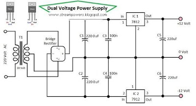
Simple Dual Voltage Power Supply 12 Volt

This is the simple circuit diagram of Dual Voltage Power Supply. It is used for Misc… application. This circuit is called regulated power supply. For this reason the main component of this circuit is Regulator IC. It also needs few components to built. The regulator 7812 is the positive voltage regulator and 7912 is the negative voltage regulator. 

Simple Dual Voltage Power Supply 12 Volt


You can also use 7809 for 9 volt positive power supply and 7909 for negative voltage power supply. It regulates voltage from 24Volt to 12 Volt (DC). The transformer input is 110Volt to 220Volt (AC) and the output must be between 12Volt to 24Volt (AC) and current must be 500mA. In this circuit some capacitors are used as a filter for removing repole.
Read More..

Saturday, October 18, 2014

LM7905 LM7805 Dual Variable Regulator power supply 5 25V

When you want Dual power supply Variable Regulator be simple. I begs for to advise this circuit, because use the integrated circuit LM7805 and LM7905. Make have Voltage +5V to +25V and -5V to -25V unless. Still pay current get about 1A enough with general usability. The important factor is you should use Transformer at enough size doesn’t lower 2A and IC all stick let off the heat with. The detail is other see in circuit picture better sir.
Read More..

Wednesday, October 15, 2014

LM317 VARIABLE POWER SUPPLY Circuit Diagram

A truly timeless circuit. LM317 is a versatile and highly efficient 1.2-37V voltage regulator that can provide up to 1.5A of current with a large heat sink. Its ideal for just about any application. This was my first workbench power supply and I still use it.

 LM317 VARIABLE POWER SUPPLY Circuit Diagram

LM317


Since LM317 is protected against short-circuit, no fuse is necessary. Thanks to automatic thermal shutdown, it will turn off if heating excessively. All in all, a very powerful (and affordable!) package, indeed.

Although LM317 is capable of delivering up to 37V, the circuit pictured here is limited to 25V for the sake of safety and simplicity. Any higher output voltage would require additional components and a larger heat sink.
Make sure that the input voltage is at least a couple of Volts higher than the desired output. Its ok to use a trimmer if youre building a fixed-voltage supply.

Possible uses:
Variable workbench power supply, fixed-voltage supply... Just about any possible application when no more than 1.5A is necessary.
Read More..

Saturday, October 11, 2014

Power Supply for USB Devices Circuit Diagram

More and more equipment is sold that runs off internal rechargeable batteries. Although a matching charger is usually supplied in the package, there are also devices that can only be charged via a USB port. That is not surprising in the case of USB MP3 players, which have to ‘dock’ in the PC anyway for some time for the purpose of file transferring. Still, the same ‘feature’ can be a serious disadvantage, for example, on ‘computer-free’ holidays. Sometimes it makes you wonder how simple the solutions to such problems actually turn out to be. After all, if it’s just a supply volt- age we’re after, then a USB port is easily imitated.
Circuit diagram :
Power Supply for USB-Devices-Circuit-Diagram
Power Supply for USB Devices Circuit Diagram 
The circuit shown here is nothing but a 7805 in a dead standard configuration. The innovation, if any, might be USB connector to which the MP3 player can be connected. The 7805 comes in different flavours — most devices can sup- ply 1 A, but there are also more advanced variants that achieve up to 1.5 A. Because a USB device is never allowed to draw more than 500 mA from the port t is plugged into, the circuit shown here should be able to supply charging and/or operating current to up to two (or three) USB devices at the same time. The input voltage may be a direct voltage of anything between 7 and 24 volts, so for use at home or abroad a simple wall cube with DC output is sufficient.
Another useful bit to make your-self might be a cable with an in-line fuse and a cigarette lighter plug so you can tap into a vehicle supply (note that this may be up to 14.4 V with a running engine). At an output current of 1 A and an input voltage of just 7 V, the 7805 already dissipates 2 watts. Assuming you’re using the most commonly seen version of the 7805, the TO-220 case with its metal tab will have a thermal resistance of about 50 °C/W. Also assuming that the ambient temperature is 20 °C, the 7805’s internal (chip) temperature will be around 120 °C. In most cases, 150 °C is the specified maximum, so ample cooling must be provided especially in a car and with relatively high input voltages. 
Read More..

Sunday, October 5, 2014

Transformerless Power Supply Circuit

Transformerless Power Supply Circuit

If you are not accomplished in ambidextrous with it, again leave this activity alone.Although Mains accessories can itself absorb a lot of current, the circuits we body to ascendancy it, usually alone crave a few milliamps. Yet the low voltage ability accumulation is frequently the better allotment of the architecture and a abundant allocation of the cost.

This ambit will accumulation up to about 20ma at 12 volts. It uses capacitive reactance instead of resistance; and it doesnt accomplish actual abundant heat.The ambit draws about 30ma AC. Always use a agglutinate and/or a aqueous resistor to be on the safe side. The ethics accustomed are alone a guide. There should be added than abundant ability accessible for timers, ablaze operated switches, temperature controllers etc, provided that you use an optical isolator as your circuits achievement device. (E.g. MOC 3010/3020) If a broadcast is unavoidable, use one with a mains voltage braid and about-face the braid application the optical isolator.C1 should be of the suppressor type; fabricated to be affiliated anon beyond the admission Mains Supply. They are about covered with the logos of several altered Safety Standards Authorities. If you charge added current, use a beyond amount capacitor; or put two in parallel; but be accurate of what you are accomplishing to the Watts. The low voltage AC is supplied by ZD1 and ZD2.

The arch rectifier can be any of the baby Round, In-line, or DIL types; or you could use four abstracted diodes. If you appetite to, you can adapt R2 and ZD3 with a 78 Series regulator. The abounding sized ones will work; but if amplitude is tight, there are some baby 100ma versions accessible in TO 92 blazon cases. They attending like a BC 547. It is additionally account acquainted that abounding baby circuits will assignment with an able supply. You can, of course, adapt any or all of the Zenner diodes in adjustment to aftermath a altered achievement voltage. As for the mains voltage, the advancement apropos the 110v adaptation is aloof that, a suggestion. I havent congenital it, so be able to agreement a little.

Read More..

Wednesday, September 24, 2014

Made Dual Regulated Power Supply


Notes:
In this circuit, the 7815 regulatates the positive supply, and the 7915 regulates the negative supply. The transformer should have a primary rating of 240/220 volts for europe, or 120 volts for North America. The centre tapped secondary coil should be rated about 18 volts at 1 amp or higher, allowing for losses in the regulator. An application for this type of circuit would be for a small regulated bench power supply.
Read More..

Tuesday, September 23, 2014

Dual Power Supply 78xx 79xx series

This is a simple dual power supply using voltage regulator IC 78xx and 79xx series. Its the best and simplest choice for most non-critical applications. The 3 terminals are input, ground and output. The 78xx & 79xx series can provide up to 1A load current and it have onchip circuitry to prevent damage in the event of over heating or excessive current.
Dual Power Supply Schematic


This dual power supply project provides a dual power supply. With the appropriate choice of transformer and 3-terminal voltage regulator pairs you can easily build a small power supply delivering up to one amp at +/- 5V, +/- 9V, +/- 12V, +/- 15V or +/-18V. You have to provide the centre tapped transformer and the 3-terminal pair of regulators you want: 7805 & 7905, 7809 & 7909, 7812 & 7912, 7815 & 7915or 7818 & 7918.

Note that the + and - regulators do not have to be matched: you can for example, use a +5v and -9V pair. However, the positive regulator must be a 78xx regulator, and the negative a 79xx one. We have built in plenty of safety into this project so it should give many years of continuous service.

These protect mainly against any back emf which may come back into the power supply when it supplies power to inductive loads. They also provide additional short circuit protection in the case that the positive output is connected by accident to the negative output. If this happened the usual current limiting shutdown in each regulator may not work as intended. The diodes will short circuit in this case and protect the 2 regulators.

Dual Power Supply Parts

 
Read More..

Monday, September 22, 2014

0 50V 2A Bench power supply circuit and description

Circuit diagram

I use the lm10 IC because it has a reference voltage and that’s useful for dc power supply. With two ICs can take different output voltage and amperage. This circuit is protected from short circuit.P2 is for controlling the current at the range of 0-2A. Stabilize the output voltage with R4 on negative pin on op-amp and with R2 & P1 on positive pin.

Op-amp output controls T1 that not let ripple of voltage.T1 increase or decrease ampere of R6 and control the voltage of T5 & T4. Pin 1 is the reference voltage and reference voltage is losing some voltage on R1 that has 100uA . This current passes through P1 too.
Vlose p1=100uA*Rp1
This lose voltage regulate output voltage rate of output current is compare between reference voltage of P3 and lose voltage on R11.T3 is protecting short circuit with R11. For reduce out put voltage to 0v should parallel one resistor 470 ohm in out put. Minimum voltage is 0.4v. The maximum output voltage is fixed with R1b and should not become over of 50v. Therefore your transformer should give 36V, 3A with 4700uF capacitor. T6, T5, T7 need heatsilk.

R1a = 2,2 K
R1b = read the text
R2 = 10 K
R3, R7 = 3.3 k
R4 = 390 Ohm
R5 = 47 K
R6 = 3.3 K 1Watt
R8 = 180 Ohm
R9, R10 = 0.47 Ohm 3Watt
R11 = 0.075 Ohm 2Watt
R12 = 470 Ohm
P1 = 500K liner potentiometer
P2 = 4.7 K potentiometer
P3 = 10 K potentiometer
C1 = 1nF
C2 = 10nF
C3 = 22nF
C4 = 47mF 63v electrolytic
C5 = 4700mF 80v electrolytic
T1, T2 = BC161
T3, T4 = BD141
T5 = BD241
T6, T7 = 2V3055
D1, D2 = 1N4148
D3, D4 = 1N4001
IC1, IC2 = LM10C


author:
e-mail: hamed_iranmehr@yahoo.com
web site: http://www.electronics-lab.com
Read More..

0 50V 2A Bench power supply circuit and explanation

Circuit diagram

I use the lm10 IC because it has a reference voltage and that’s useful for dc power supply. With two ICs can take different output voltage and amperage. This circuit is protected from short circuit.P2 is for controlling the current at the range of 0-2A. Stabilize the output voltage with R4 on negative pin on op-amp and with R2 & P1 on positive pin.

Op-amp output controls T1 that not let ripple of voltage.T1 increase or decrease ampere of R6 and control the voltage of T5 & T4. Pin 1 is the reference voltage and reference voltage is losing some voltage on R1 that has 100uA . This current passes through P1 too.
Vlose p1=100uA*Rp1
This lose voltage regulate output voltage rate of output current is compare between reference voltage of P3 and lose voltage on R11.T3 is protecting short circuit with R11. For reduce out put voltage to 0v should parallel one resistor 470 ohm in out put. Minimum voltage is 0.4v. The maximum output voltage is fixed with R1b and should not become over of 50v. Therefore your transformer should give 36V, 3A with 4700uF capacitor. T6, T5, T7 need heatsilk.

https://blogger.googleusercontent.com/img/b/R29vZ2xl/AVvXsEiNGUJz3xFyTeOWzRrgTX8RUulvTDBXw1UStuUvCw6hSd-Bigs8zfI6YuiIcmvzu-bTwQWts80M5COP4NIg35NLIx4t8Cm6my8ZZ0PaJ2YpgEmoy8C7lW0FYQoFEShbb2JPV_f5plkpWqdg/s1600/Simple+0-50V+2A+Bench+Power+Supply+Circuit+Diagram.jpg

R1a = 2,2 K
R1b = read the text
R2 = 10 K
R3, R7 = 3.3 k
R4 = 390 Ohm
R5 = 47 K
R6 = 3.3 K 1Watt
R8 = 180 Ohm
R9, R10 = 0.47 Ohm 3Watt
R11 = 0.075 Ohm 2Watt
R12 = 470 Ohm
P1 = 500K liner potentiometer
P2 = 4.7 K potentiometer
P3 = 10 K potentiometer
C1 = 1nF
C2 = 10nF
C3 = 22nF
C4 = 47mF 63v electrolytic
C5 = 4700mF 80v electrolytic
T1, T2 = BC161
T3, T4 = BD141
T5 = BD241
T6, T7 = 2V3055
D1, D2 = 1N4148
D3, D4 = 1N4001
IC1, IC2 = LM10C


author:
e-mail: hamed_iranmehr@yahoo.com
web site: http://www.electronics-lab.com
Read More..

Saturday, September 20, 2014

TL594 12V DC Switch Mode Power Supply Wiring diagram Schematic

In recent years, the use of switch mode power supply (SMPS) has become more comon as more applications demand for greater power eficiency. It makes use of semiconductor (mostly MOSFET) fast switches to switch DC input that has been rectified at high frequency. The advantages of high frequency switching are that it reduces the size of inductor, capacitors & transformer used. Other advantages of switching power supply over linear power supply are :

1) High Efficiency (up to 90% and above for nice design).
2) Output can be higher than input.
3) Able to operate over a variety of input power supply.
4) Able to have over output.

The setback of using SMPS compared to linear power supply is that it generates electrical noise which contributes to electromagnetic compatibility design issues & more part count.

Buck Converter SMPS
The SMPS schema below from Power Integration makes use of LNK304 as its high frequency switch. Take note that this schema is non isolated type which means that the output is not electrically isolated from the input & all testing ought to be completed using an isolation transformer to provide the AC line input to the board.

Make positive that you have electrical safety knowledge & experience before you embark on doing this project.

12V DC Switch Mode Power Supply Circuit Diagram

12V


Read More..