Showing posts with label for. Show all posts

Friday, November 14, 2014

How to Build a UPS for USB devices

Portable systems often include circuitry that derives power from an external source, such as USB. When the system disconnects from the USB supply, a battery takes over and supplies current via a dc/dc converter. A diode-OR connection (Figure 1 offers the easiest way to ensure that the supply voltage doesnt sag during this switchover to the battery. The diodes forward voltage drop, however, can reduce battery life and efficiency.

A diode-OR connection is effective but lossy.


 A boost-converter circuit is an improvement over the simple diode-OR connection.

The single-cell, boost-converter circuit with external PFET (Figure 2) is an improvement over the diode-OR connection. The PFET, Q1, coupled with IC1s internal gain block, forms a linear regulator. The USB power supply has a diode-OR connection to Q1s source. Setting the boost converters output to 3.4V allows the drain of Q1 to regulate to 3.3V. This configuration produces negligible loss in Q1. The bus-supply voltage available to USB devices ranges from 4.4 to 5.25V.

When you connect the bus, it forward-biases D1 and causes the boost converter to idle. The converter continues to idle as long as its output remains above the 3.4V regulation point. The bus supply serves the load and activates the current source to charge the battery.


Adjusting R1 allows you to set the current-source output to charge the nickel-metal-hydride cells at a level one-tenth the batterys capacity. Disconnecting the circuit from the USB supply causes the boost converter to cease idling and supply current to the load via the battery. Figure 3 shows that the load current suffers no interruption during a switchover from USB to battery.
Read More..

Thursday, November 6, 2014

RF detector circuit for High Frequency

Often we need to see which is ideal for the placement of an antenna, a transmitter or other device for high frequency where its signal can reach and where it leaves point. For this we can use a detector circuit, also called the sniffer, which is tuned to the operating frequency of the desired system. This detector is described in this article is very simple to operate and do, just uses two diodes and two transistors and a half dozen passive components, their frequency of detection is around 2.2Ghz and its sensitivity is pretty good.

RF detector circuit for High Frequency


Its operation is simple, the transistors Q1 and Q2 are BFS17 are being used with RF amplifiers. LED1 can be replaced by a VU to have greater precision in signal check. The circuit has a very broad frequency tuned, it will capture RF signals from microwaves, cell phones, WIFI, etc.. I believe that the transistor can be replaced by BFS17 BRF92 or BFG591, which are easier to find here.

Detector RF High Frequency

The circuit must be mounted in a metal box to minimize capacitive effects of hand and other external interference, only the antenna must be out of caixa.Para test the detector, as you approach a signal source, the 1 LED gets brighter. The simplicity of the circuit, for sure it will capture unwanted signals, especially harmonics powerful transmitters, but is still reliable equipment.
Read More..

Wednesday, November 5, 2014

Always on for PCs

Many enthusiasts will be using their PCs as data loggers, controllers or as web servers. ln these cases it is important that  the machine is kept powered up for as great a fraction of the time as possible, even if there has been a power cut or if the power button is inadvertently pressed by another member of the household. Todays operating systems offer a range  of automation options and it is perfectly possible to arrange things so that the computer starts itself up automatically.

Always on for PCs Circuit diagram :


Always


The always oncircuit shown here automatically restarts an ATX PC in the above situations. There are just two components: a Schottky diode connecting the power but-ton pin on the motherboard to the +5 V line on the power supply, and a capacitor from the power  button pin to ground. The  capacitor  is a 68  pF tantalum type rated at 6.3 V, and the diode is a type SB 120, rated at 20 V and 1 A. The total component cost is in the sub-one-beer range!

The most convenient arrangement is to mount the circuit directly on a 4-way Molex disk drive power plug, insulating the capacitor and diode using heatshrink tubing. The assembly can then be plugged  into a spare socket on the power  supply.

The operation of the circuit is straightforward. When the +5 V supply fails (i.e., when the computer is turned off), the  power button pin on the motherboard is pulled low via the Schottky diode. This instructs the motherboard to power up again. As long as the +5  V supply is present, the diode blocks and the power button pin remains at high impedance, floating typically at around 3.3 V. The capacitor serves to filter out spikes and brief dropouts. ln its simpler version  the circuit replaces the power button on the case, and the computer can now only be switched on and off at the mains.

The author has tested the circuit on modern SuperMicro X8SAX and XSDTH-6F mother-boards as well as on an olderTyan  Tiger MPX. He found that the capacitor value should be reduced in some cases: the SuperMicro motherboards have a high internal pull-up  resistance which only charges the capacitor rather slowly.

Note that some PC keyboards have a Sleep button which puts the computer into a low-power mode. ln this case the  circuit will not work, and you should either use a keyboard without such a button or disable sleep modes from within  the operating system.  ln its more advanced version the existing power button is retained in parallel with the circuit (see circuit diagram). The power button then  causes a graceful  shutdown whereby the operating system can bring the computer to a halt in an orderly manner.

Source : http://www.ecircuitslab.com/2012/06/always-on-for-pcs-circuit.html

Read More..

Friday, October 31, 2014

Universal Battery Charger Battery charger for general purpose usage Universal Battery Charger circuit diagram The chargers output voltage is adjust

Universal Battery Charger

Battery charger for general purpose usage.

Universal
The chargers output voltage is adjustable and regulated, and has an adjustable constant-current charging circuit that makes it easy to use with most NiCad batteries. The charger can charge a single cell or a number of series-connected cells up to a maximum of 18V.

Power transistors Q1 and Q2 are connected as series regulators to control the battery chargers output voltage and charge-current rate. An LM-317 adjustable voltage regulator supplies the drive signal to the bases of power transistor Q1 and Q2. Potensiometer R9 sets the output-voltage level. A current sampling resistor, R8 (a 0.1 ohm/5W unit), is connected between the negative output lead and circuit ground. For each amp of charging current that flows through R8, a 100mV output is developed across it. The voltage developed across R8 is fed to one input of comparator U3. The other input of the comparator is connected to variable resistor R10.

As the charging voltage across the battery begins to drop, the current through R8 decrease. Then the voltage feeding pin 5 of U3 decreases, and the comparator output follows, turning Q3 back off, which completes the signals circular path to regulate the batterys charging current.

The charging current can be set by adjusting R10 for the desired current. The circuits output voltage is set by R9
Read More..

Inverter Circuit for Soldering Iron

The following inverter circuit can be used to supply soldering iron or other small electronic devices which need up to about 50W / 230V power supply.

Inverter


Transistors T1 and T2 (each BC547) form an astable multivibrator that creates 50Hz signal. The complementary outputs from the collectors of transistors T1 and T2 are fed to pnp Darlington driver stages formed by transistor pairs T3-T5 and T4-T6 (utilising BC558 and BD140). The outputs from the drivers are fed to transistors T7 and T8 (each and every 2N3055) connected for push-pull operation. Use suitable heat-sinks for transistors T5 via T8.

A 230V AC primary to 12V-0-12V, 4.5A secondary transformer (X1) is utilised. The centre-tapped terminal of the secondary of the transformer is connected to the battery (12V, 7Ah), whilst the other two terminals of the secondary are connected to the collectors of power transistors T7 and T8, respectively.

Whenever you power the circuit making use of switch S1, transformer X1 produces 230V AC at its primary terminal. This voltage could be employed to heat your soldering iron.

Build the circuit on a standard purpose PCB and place it in a suitable cabinet. Hook up the battery and transformer with proper current-carrying wires. On the front panel of the box, fit power switch S1 along with a 3-pin socket for connecting the soldering iron.

Note that the ratings of the battery, transistors T7 and T8, and transformer could vary as these all depend on the load (soldering iron).
Read More..

Sunday, October 26, 2014

A Frequency Doubler Effect for Electric Guitar


This circuit is a octave shifting that is used for electric guitar is done by rectifying the original signal, just like AC to DC conversion inside your AC-DC power supply adapter. This circuit is use single supply instead of symmetric power supply. This is the figure of the circuit.
The rectifying is done by four 1N4148 silicon diodes, configured as full-wave rectifier bridges. Because the bridge is inserted inside the negative feedback of the operational amplifier (op-amp) U1B, the nonlinear characteristic of the diodes around the turn-on point (the forward bias voltage) is compensated by the op-amp’s feedback mechanism. 
Read More..

Friday, October 17, 2014

Electrical Isolation For I2C Bus

When the SDA (Serial DAta) lines on both the left and right lines are 1, the circuit is quiescent and optoisolators IC1 and IC2 are not actuated. When the SDA line at the left becomes 0, current flows through the LED in IC1 via R2. The SDA line at the right is then pulled low via D2 and IC1. Optoisolator IC2 does not transfer this 0 to the left, because the polarity of the LED in IC2 is the wrong way around for this level. This arrangement prevents the circuit holding itself in the 0 state for ever. As is seen, the circuit is symmetrical. So, when the SDA line at the right is 0, this is transferred to the left. The lower part of the diagram, intended for the SCL (Serial CLock) line, is identical to the upper part.

Electrical Isolation For I2C Bus Circuit diagram :


 Electrical Isolation For I2C Bus Circuit Diagram

Resistors R1, R4, R5, and R8, are the usual 3.3 kΩ pull-up resistors that are obligatory in each I2C line. If these resistors are already present elsewhere in the system, they may be omitted here. The current drawn by the circuit is slightly larger than usual since the pull-up resistors are shunted by the LEDs in the optoisolators and their series resistors. Nevertheless, it remains within the norms laid down in the I2C specification.
Read More..

Time Delay Circuit for Relay

Often we need a timer circuit which delays an action, eg the activation of a device through a relay. We call this delay circuit for driving relay. We use the relay in most cases by the versatility of its use, we can make a drive circuit using 12 volts DC to power a device 110 or 220 Volts AC, with any current since the relay contacts support. Relays are electrically operated switches, so it works as a common key. Timed relay or commercial Delay


Timed


Relays ON-delay,? after energizing the relay initiates the timing, in which sophisticated models have an external adjustment via a potentiometer or selector switch. After the expiration of the predetermined time by the user to the switching contacts. Industrial relays are in their majority.

The pneumatic relay delay

Some relays comes with this "delay " , are called timed relays , the former has a kind of " buffer" mechanism , when the coil is energized or not energized . These mechanisms used pneumatic dampers or piston systems with cylinder filled with liquid for shock absorption necessary to slow the movement of the armature . This addition gives the relay delay time of activation, call delay .

The delay relay solid state

The current time delay relays use electronic to generate a time interval circuits , and then energize the relay coil . The electronic timer relays are more versatile than , less prone to failure and time variations with wear mechanical / pneumatic models .

Use timed relay or delay

The use of relays timed or delay is very comprehensive in the industry or even residential , are some utilities to use this device.

As time delay fuse , is a special type of fuse that is designed for specific applications where a delay for shutdown is necessary. It is used in machinery or equipment that consume power surges when connected or give matches , but while using their consumption drop dramatically .

Switch controls two time delay relays are used in conjunction to provide a constant frequency on and off , for sending intermittent power to machines or devices .

Control security wipe before a door of a gas chamber be safely released , an exhaust system must be connected for a certain period of time to " clean up" the chamber of any fumes , poisonous gases , flammable or explosives. A time delay relay in such control provides the time required for cleaning.

Soften the departure of engines , instead of starting in large electric motors , giving full force from the neutral , we can start with low voltage so the engine will be started more smoothly and with less starting current. After a time interval the total energy is applied. See More on relays

Trigger conveyor in sequence , when multiple conveyor belts are arranged to transport material, the straps should be started in the reverse order ( the last before the first ) so that the material does not stack . In order to obtain maximum speed, sometime a circuit delay may be needed on each conveyor belt to give you enough time to reach the speed before being fed time.

The two types of basic delay relays ( on or off )

Basically there are two types of delays relays, DelayRelay On Time and Off Time DelayRelay , ie a relay with delay to turn off and another relay with time- delayed to connect . The relay late to call, or time delay relay On is the most widely used and is referred to most of this text , and also when we talk about delay switch or time delay .


How to delay the electronic signal - Relay Delay Time Homemade


Relay circuit to late to turn, or time delay relay On

Relay


First we see a relay circuit to late to turn, or time delay relay on. To delay a pulse we use a timer or timer, it is called Time Delay circuit should work delaying the activation of the relay, so we will have our relay time delay (time Delay Relay). This circuit delay time for relay can be used in most commercially available relays which has a DC voltage of 12 volts and has a coil resistance of 75 ohms or more.

Its operation is simple , when the circuit is energized resistor R2 connected across the supply provides a discharge path for the capacitor when the power is off , the discharge takes advantage of the breakdown voltage Emitter - base of a bipolar transistor . The base junction - reverse emitter connected transistor 2N3904 is used as a zener diode 8 volts that creates a higher turn on voltage for the transistors connected in Darlington configuration that trigger the relay .

In Q3 any bi-polar transistor may be used, but the zener voltage will range from about 6 to 9 volts, depending upon the transistor used. The time delay is 7 seconds , that using a 47K resistor R1 and a capacitor C1 100uF . To reduce the time delay relay simply decreasing the values ​​of R1 and C1. For longer periods of delay , ie to increase the time delay , should place a capacitor with the largest value C1 , the resistor R1 should not be increased.

List of Contents

R1 - Resistor 10 K Ohms 1/4 Watt
R2 - Resistor 47 K Ohms 1/4 Watt
C1 - Electrolytic Capacitor 100uf x 25 Volts
D1 - 1N4001 diode
Q1 - Transistor 2n3052
Q3 and Q2 - 2N3904 transistor
RY1 - Relay 12 Volts

Circuit to relay off delay, or time delay relay Off

Circuit


The circuit slows down the opening of the relay contacts a short period of time after voltage interruption. The circuit is very simple, a capacitor C1 is charged and the relay is closed when the voltage at the anode of diode D2 rises to 12 volts.

When the voltage is cut off the relay will stay on until the capacitor C1 is fully discharged. The delay time depends on the value of the capacitor, the relay coil current and transistor gain. So to avoid calculations can go testing electrolytic capacitors to obtain the desired delay time.

List of Contents

C1 Electrolytic Capacitor 100uf x 25 Volts
Diode D1 1N4001
D2 Diode 1n4882
Q1 - Transistor 2N2222
RY1 - Relay 12 Volts
Read More..

Thursday, October 16, 2014

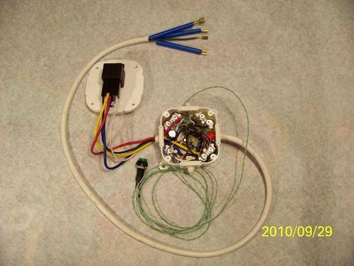
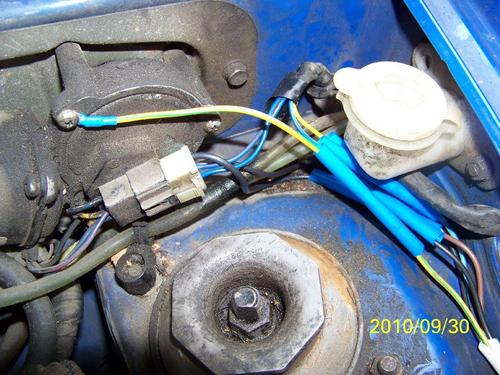
Hacking Car Wipers for Easy Control

How do you want to have your wipers become more intelligent? In this way, they could remember how frequent you need to use them. But of course, this will need the help of an ATmega8L micro-controller.

Hacks and Mods: Hacking Car Wipers for Easy Control

When you need to activate the wiper, you just press the button and it will run in one course. There is a 45 seconds waiting time that if you do not press the button, it will go on standby while telling itself that only one course is needed. The system will activate the wiper again if the button is pressed before 45 seconds. The good thing is that it will remember the interval when you pressed the button.

Hacks and Mods: Hacking Car Wipers for Easy Control
Read More..

How to Lights Control for Model Cars

The author gave his partner a radio controlled (RC) model car as a gif t. She found it a lot of fun, but thought that adding realistic lights would be a definite improvement. So the author went back to his shed, plugged in his soldering iron, and set to work equipping the car with realistic indicators, headlights, tail lights and brake lights.

Lights Control for Model Cars Circuit Diagram

The basic idea was to tap into the signal from the radio control receiver and, with a bit of help from a microcontroller, simulate indicators using flashing yellow LEDs and brake lights using red LEDs. Further red LEDs are used for the tail lights, and white LEDs for the headlights. Connectors JP4 and JP5 (channel 0) are wired in parallel, as are JP6 and JP7 (channel 1), allowing the circuit to be inserted into the servo control cables for the steering and drive motor respectively. The ATtiny45 micro-controller takes power from the radio receiver via diode D1. T1 and T2 buffer the servo signals to protect IC1’s inputs from damage. 
IC1 analyses the PWM servo signals and gen-erates suitable outputs to switch the LEDs via the driver transistors. T3 drives the two left indicators (yellow), T4 the two right indica-tors, and T5 the brake LEDs (red). The red tail lights (JP2-8 and JP2-8) and the white head-lights (JP2-9 and JP2-10) are lit continuously. The brake lights are driven with a full 20 mA, so that they are noticeably brighter than the tail lights, which only receive 5 mA. If you wish to combine the functions of tail light and brake light, saving t wo red LEDs, sim-ply connect pin 10 of JP2 to pin 14 and pin 12 to pin 16. Then connect the two combined brake/tail LEDs either at JP2-5 and JP2-6 or at JP2-7 and JP2-8.

JP3 is provided to allow the use of a separate lighting supply. This can either be connected to an additional four-cell battery pack or to the main supply for the drive motor. The val-ues given for resistors R8 to R17 are suitable for use with a 4.8 V supply. JP2 can take the form of a 2x10 header.

As usual the sof t ware is available as a free download from the Elektor web pages accom-panying this article[1], and ready-programmed microcontrollers are also available. The microcontroller must be taught what servo signals correspond to left and right turns, and to full throttle and full braking. First connect the fin-ished circuit to the radio control electronics in the car, making sure everything is switched of f. Fit jumper JP1 to enable configuration mode, switch on the radio control transmit-ter, set all proportional controls to their cen-tre positions, and then switch on the receiver. The indicator LEDs should first flash on both sides. Then the car will indicate left for 3 s: during this time quickly turn the steering on the radio control transmitter fully to the left and the throt tle to full reverse (maximum braking).

Hold the controls in this position until the car starts to indicate right. Then set the controls to their opposite extremes and hold them there until both sides flash again. Now, if the car has an internal combustion engine (and so cannot go in reverse), keep the throttle control on full; if the car has an electric motor, set the throttle to full reverse. Hold this position while both sides are flashing.  
Read More..

Saturday, October 11, 2014

Power Supply for USB Devices Circuit Diagram

More and more equipment is sold that runs off internal rechargeable batteries. Although a matching charger is usually supplied in the package, there are also devices that can only be charged via a USB port. That is not surprising in the case of USB MP3 players, which have to ‘dock’ in the PC anyway for some time for the purpose of file transferring. Still, the same ‘feature’ can be a serious disadvantage, for example, on ‘computer-free’ holidays. Sometimes it makes you wonder how simple the solutions to such problems actually turn out to be. After all, if it’s just a supply volt- age we’re after, then a USB port is easily imitated.
Circuit diagram :
Power Supply for USB-Devices-Circuit-Diagram
Power Supply for USB Devices Circuit Diagram 
The circuit shown here is nothing but a 7805 in a dead standard configuration. The innovation, if any, might be USB connector to which the MP3 player can be connected. The 7805 comes in different flavours — most devices can sup- ply 1 A, but there are also more advanced variants that achieve up to 1.5 A. Because a USB device is never allowed to draw more than 500 mA from the port t is plugged into, the circuit shown here should be able to supply charging and/or operating current to up to two (or three) USB devices at the same time. The input voltage may be a direct voltage of anything between 7 and 24 volts, so for use at home or abroad a simple wall cube with DC output is sufficient.
Another useful bit to make your-self might be a cable with an in-line fuse and a cigarette lighter plug so you can tap into a vehicle supply (note that this may be up to 14.4 V with a running engine). At an output current of 1 A and an input voltage of just 7 V, the 7805 already dissipates 2 watts. Assuming you’re using the most commonly seen version of the 7805, the TO-220 case with its metal tab will have a thermal resistance of about 50 °C/W. Also assuming that the ambient temperature is 20 °C, the 7805’s internal (chip) temperature will be around 120 °C. In most cases, 150 °C is the specified maximum, so ample cooling must be provided especially in a car and with relatively high input voltages. 
Read More..

Thursday, September 25, 2014

Electronic Load Circuit for Testing Power Supplies

For testing power supplies and transformers, an appropriate, preferably adjustable, load is indispensable. Often, a number of interlinked high-wattage resistors are used for this purpose, but that is not alway satisfactory, feasible or safe. The electronic load described here is a much more flexible and suitable solution.

The load is based on a number of power transistors. The output current, which is the sum of the collector currents of these transistors, is converted into heat that is lost by convection and radiation through a suitable heat sink. The base current of the transistors is arranged at a value that results in the required level of emitter-collector current. Since the base-emitter voltage that deter- mines the base current of a transistor varies with temperature (¤ 2-8 mV / °C), an opamp is used to iron out any consequent variations of the base current. The end result is an adjustable load with a ’resistance’ value ranging from almost zero to infinity and a thermal rating that depends solely on the power transistors and the manner in which these are cooled. The load may operate in either the constant-current mode or the constant resistance mode. In the first, the current remains constant irrespective of the applied voltage, while in the second it is directly proportional to the applied voltage. A waveform generator (triangular, sinusoidal and rectangular) enables the ’resistance’ to be modulated.  

Circuit description

Each of the power transistors, T3-T7, in Fig. 1 can draw a collector current of up to 2 A with an appropriate heat sink. Resis- tors R24—R33 provide a measure of current feedback, which ensures equalization of the currents drawn by the individual power transistors.

Resistance simulation

Each group of power transistors, T3—T7 and T8—T12 respectively, is driven by one half of dual opamp IC2 via a driver transis- tor, T1 and T2 respectively. The inverting input of the opamps is connected to the emitter resistor of the first power transistor in each group. The non- inverting inputs are connected in parallel and linked to the pole of switch Sib. This pole receives one of four different control signals via the switch contacts.

When S1 is in position l (7), terminal "P” carries part of the voltage, as set by P2- R9, that exists between terminal "U" and earth. The opamp tries to reduce the ‘potential difference between its inputs to vir- tually zero. It will therefore increase the base currents of the power transistors, and thus the load current, until the voltage drop across R24 (R29) and the input voltage set by P2 are equal. When the input voltage rises, the potential at the non-inverting in- puts, and thus the load current, increases. This means that the circuit behaves as a resistance, the value of which may be set with the aid of P2.

Modulation and constant current

Opamps IC1a and IC1b form a simple function generator that produces rectangular waveforms when S1 is in position 2 (8) and triangular waveforms when the switch is in position 3 (9). The frequency is adjustable over the range 5-50 Hz by P3. The signal from the generator is amplified in ICM and fed, via SIB and "P", to the non·inverting inputs of control amplifier IC2 where it serves as reference voltage. Since this potential is no longer dependent on the input voltage to the load, an in- crease in the input level no longer leads to a higher load current. In fact, if the signal, whether triangular or rectangular, is used as the control signal, the circuit functions as a modulated constant-current source.

The load current is modulated in the same way as the control signal. The gain of IC1d, which determines the depth of modulation, is set by P1. Potentiometer P4 enables an offset to be added to the control sign al. This offset makes it possible to shift the modulation level with respect to zero. ln other words, P1 sets the level by which the current varies, while P4 determines between which values modulation is effected, for resistance, between 2.5 A and 3.0 A. This assumes, of course, that the unit or device under test can provide currents at those levels .

External modulation

 Opamp IC1e serves as an inverting. unity-gain amplifier. Its output signal B available at contact 4 of Si. It may be fed with an external modulating signal via Ki. The input must be between 0 V and +10V. The con- trol characteristic may be set between 3 A / V and 1.5 A / V for each power transistor. If, for example, the voltage at K1 changes by 100 mV, the output current varies by 3 A with P1 set to maximum and by 1.5 A with Pi set to minimum.

Construction and alignment

The load is best built on the PCB shown in Fig. 2. This figure does not show the part of the board for power transistors T8—T12 and associated components since this is identical to that for T3—T7. Before any start can be made with populating, the board must be cut into four with a fine hacksaw. Screw each of the two long parts to a 5 mm thick aluminium bracket. Since the collectors of the power transistors will be at the same potential, there is no need for insulating washers, provided. that the heat sinks and aluminium brackets are isolated from the enclosure.

Do not fit the emitter resistors too close A to the board, because even in normal operation these get fairly hot. The same applies to R22 and Rza. The choice of enclosure depends in the first instance on the heat sinks used. The requirements of these are fairly stringent because they have to dissipate some 300 W. The dissipation may be increased to 1 kW if forced cooling is used. The only calibration is in the provision of a scale for P2. For that purpose, a laboratory ype power supply with variable output and capable of providing an output current of at least a few amperes is required. Measure the voltage and current for a number of positions of P2 and calculate the corresponding resistance. The resulting scale is linear for input voltages greater than about 4 V

Fit the potiometers and switch On the front panel of the enclosure together with two heavy-duty, spring- loaded, insulated terminals. Connect points "U" and "T" to their positive terminals, and the earth points to the negative terminal. To ensure that sufficient current flows through the power transistors, the load needs its own 12 V power supply, for which a simple unit with a 500 mA transformer and a Type 7812 voltage regulator will do fine.

 The maximum values the power - transistors can tolerate are not those found in their data sheet, that is, 60 V 15 A, 115 W. Instead, the maxi- mum dissipation is determined from the safe operating area (SOA) shown in Fig. 3. This shows that the maximum collector current de- creases with a rising collector-emitter volt- age. Conversely, when a current of 15 A flows through the transistor, its collector- emitter voltage should not exceed 8 V It is imperative that at no time the C—E voltage exceed the limit for a given current and vice versa. But that is not all. The SOA characteristic in Fig. 3 refers to a maxi- mum dissipation of 115 W at a case tem- perature of 25°C. With rising temperature, the dissipation is degraded at a rate of 0.65 W/°C. This means that at a case tempera- ture of 80 OC the maximum dissipation is only 80 W and at 140 °C it is only 40 W.

The design of the load allows for each power transistor to tolerate a current of up to 2 A, so that the input voltage can go up to close to 60 V. lf that is not sufficient, the ZN3055 transistors should be re- placed by types with a higher rating.

Read More..

Sunday, September 21, 2014

Solar Charger for Lead Acid Batteries

This circuit is still under development, but works well as shown.

This circuit is intended for charging lead-acid batteries with a solar panel. The customary diode that prevents the battery from discharging through the solar panel has been replaced by a FET-comparator combination. The charger will stop charging once a pre-set voltage (temperature compensated) has been reached, and recommence charging when the voltage has dropped off sufficiently. The load is disconnected when the baterry voltage drops below 11V and reconnected when it gets back to 12.5V.

The circuit has the following features:

  •     Charges until Vbat = 13,8V (adjustable), then float charges;
  •     Shuts down load when Vbat <11v (adjustable), resets at 12,5v;
  •     Temperature compensation;
  •     Will work with cheap and readily available components like LM393 comparators and BUZ11 FETs;
  •     Uses less than 1.3mA (Attempts to use micropower comparators have failed spectacularly so far, see below);
  •     Burns less than 20mW in FETs when charging at 0,5A. (More expensive FETs with a lower RDSON will yield even better results).
  • Note that the charging current is limited only by the solar panel used.

    Heres the circuit:

    Solar

    Note the funny place of grounding of the first 2 comparators. Theres some weirdness here: this bit of the circuit gives me headaches. Two problems:

    •     If I ground the first two comparators (LM393) in the same place as the third, i.e. not between the FETs, the thing wont work and the battery will discharge over the solar panel. Why? Am I playing to close to the rails? How can this be remedied/improved/redesigned? Do I need a diode between the comparators imputs?
    •     If I use micropower comparators like the Texas Instruments TLC393, the comparators blow up spectacularly, but with the standard LM393 everything works fine. Why? What did I miss?

    Help would be greatly appreciated!

    Next attempt

    This one works fine and uses about 0.5mA, but that might improve because Im not done tweeking yet:

    Solar

    by Oscar den Uijl, odu@xs4all.nl

Read More..

Thursday, September 18, 2014

Reuse Old Mobile Phone Battery for LED lighting

Normally mobile batteries have a lifespan of 2-5 years under normal usage. But then we have to replace them. Nowadays there are cheap replacement batteries which cost no more than 1$. But these low cost batteries run only 6-12 months. What to do with the used batteries, which can’t be reused in mobiles? Well, easy solution is to use the batteries in a circuit that requires less current. We can use them for LED lighting.

Do you have old unusable Mobile battery?
Hacks and Mods: Reuse Old Mobile Phone Battery for LED lighting
Normally mobile batteries have a lifespan of 2-5 years under normal usage. But then we have to replace them. Nowadays there are cheap replacement batteries which cost no more than 1$. But these low cost batteries run only 6-12 months. What to do with the used batteries, which can’t be reused in mobiles?
Hacks and Mods: Reuse Old Mobile Phone Battery for LED lighting
Well, easy solution is to use the batteries in a circuit that requires less current. We can use them for LED lighting. Thus your automatic lighting emergency light is ready which runs by your waste Mobile Battery. 


Source by : http://www.extremecircuits.net/2012/08/hacks-and-mods-reuse-old-mobile-phone.html
Read More..

Thursday, September 11, 2014

Brightness controller circuit diagram for your car


This is brightness controller schema diagram.You can use this schema for your car or for your bike.Here I have used famous IC NE 555.


Note

# Use 6V bulbs with this

# Build this schema on a pcb.
Read More..

Sunday, September 7, 2014

USB Charger For Lithium Ion battery

USB
USB Battery Charger For Lithium Ion battery with the LM3622 is a series of lithium ion battery charger. This charger circuit operates using power from the USB source PC.
Read more
Read More..

Saturday, September 6, 2014

Modem for Digital Modes Circuits Wiring diagram

Ham Com is a modem for almost all types of digital transmission for radio amateurs. It can be used to RTTY, ASCII, NevTex, Sitor, Amtor, Fec, CW, FSK, etc.. The modem is simple and can even be used for receiving faxes and SSTV wx-using JV-FAX software.

 Modem for Digital Modes Circuits Diagram

Modem


To use this modem, you need a PC with serial port, Software HamCom and radio equipment.
Read More..

Wednesday, September 3, 2014

TDA2822 made for 5 1 audio amplifier system

Skema Rangkaian Circuit combination of the 3 IC TDA2822  above can be used for 5.1 audio power amplifier system with low power output . The input signal used is analog signal not digital (SPDIF) , so it needed some input to the jack input. The speakers are suitable for use have impedance 8 Ohms , and with power 4 Watt, to Left , Right , Rear pair , center , and subwoofer speakers. To run this circuit , is also required circuit for volume control as tone control.


Component and technical Information :
C1-C6 : 220uF/25V
C7-C9 : 47uF/16 V
IC       : TDA2822 x3
CON-1: VCC +12volts DC
CON-2: Ground
CON-3: Left Speaker
CON-4: Right Speaker
CON-5: Rear Speaker
CON-6: Rear Speaker
CON-7: Center Speaker
CON-8: Subwoofer Speaker
X1-1:Ground
X1-2:Subwoofer Input
X1-3:Center Input
X1-4:Rear Input
X1-5:Rear Input
X1-6:Right Input
X1-7:Left Input

See this Printed circuit board below:

circuit and PCB Design use Cadsoft Eagle Software
Read More..

Sunday, August 31, 2014

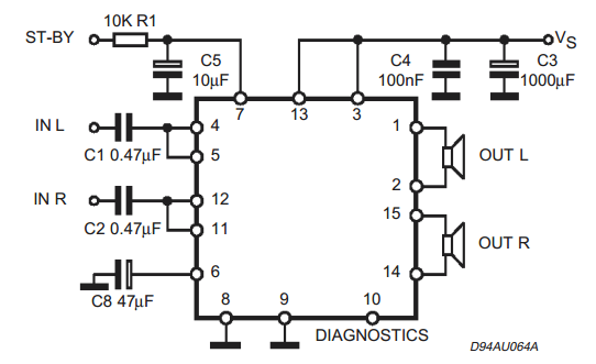
2x30W DUAL QUAD POWER AMPLIFIER FOR CAR RADIO TDA7377

Features:

  • HIGH OUTPUT POWER CAPABILITY:
  • 2 x 35W max./4Ω
  • 2 x30W/4Ω EIAJ
  • 2 x30W/4Ω EIAJ
  • 2 x 20W/4Ω @14.4V, 1KHz, 10%
  • 4 x 6W/4Ω @14.4V,1KHz, 10%
  • 4 x 10W/2Ω @14.4V, 1KHz, 10%
  • MINIMUM EXTERNAL COMPONENTS
  • COUNT:
  • – NO BOOTSTRAP CAPACITORS
  • – NO BOUCHEROT CELLS
  • – INTERNALLY FIXED GAIN (26dB BTL)
  • ST-BY FUNCTION (CMOS COMPATIBLE)
  • NOAUDIBLEPOPDURINGST-BYOPERATIONS
  • DIAGNOSTICS FACILITY FOR:
  • – CLIPPING
  • – OUT TO GND SHORT
  • – OUT TO VS SHORT
  • – SOFT SHORT AT TURN-ON
  • – THERMAL SHUTDOWN PROXIMITY
  • Protections:
  • OUPUT AC/DC SHORT CIRCUIT
  • – TO GND
  • – TO VS
  • – ACROSS THE LOAD
  • SOFT SHORT AT TURN-ON
  • OVERRATING CHIP TEMPERATURE WITH
  • SOFT THERMAL LIMITER
  • LOAD DUMP VOLTAGE SURGE
  • VERY INDUCTIVE LOADS
  • FORTUITOUS OPEN GND
  • REVERSED BATTERY
  • ESD
Circuit Diagram:
2x30W DUAL AMPLIFIER aplication circuit

2x30W QUAD AMPLIFIER aplication circuit

Read More..