Thursday, November 13, 2014
ADV7123 Digital to Analog Converter Connection Diagram and Datasheet

This digital-to-analog converter (DAC) integrated circuit is designed for lowest noise performance, both radiated and conducted noise. A recommended connection diagram for the ADV7123 is shown in the following schematic diagram.
According to the ADV7123 datasheet, this device consists of three high speed, 10-bit, video DACs with complementary outputs, a standard TTL input interface, and a high impedance, analog output current source. It used to be applied in digital video systems, image processing, digital radio modulation, color graphics and more.
Additional information on ADV7123 Digital-to-Analog Converter Connection Diagram can be seen in this datasheet of pdf filetype (source: analog.com).

Wednesday, November 12, 2014
12V Speed Dimmer Controller Diagram Circuit
SILICON CHIP has produced a number of DC speed controllers over the years, the most recent being our high-power 24V 40A design featured in the March & April 2008 issues. Another very popular design is our 12V/24V 20A design featured in the June 1997 issue and we have also featured a number of reversible 12V designs.Circuit looks like:
For many applications though, most of these designs are over-kill and a much simpler circuit will suffice. Which is why we are presenting this basic design which uses a 7555 timer IC, a Mosfet and not much else. Being a simple design, it does not monitor motor back-EMF to provide improved speed regulation and nor does it have any fancy overload protection apart from a fuse. However, it is a very efficient circuit and the kit cost is quite low.Parts layout:
There are many applications for this circuit which will all be based on 12V motors, fans or lamps. You can use it in cars, boats, and recreational vehicles, in model boats and model railways and so on. Want to control a 12V fan in a car, caravan or computer? This circuit will do it for you.Circuit diagram:
The circuit uses a 7555 timer (IC1) to generate variable width pulses at about 210Hz. This drives Mosfet Q3 (via transistors Q1 & Q2) to control the speed of a motor or to dim an incandescent lamp.Halogen lamps:While the circuit can dim 12V halogen lamps, we should point out that dimming halogen lamps is very wasteful. In situations where you need dimmable 12V lamps, you will be much better off substituting 12V LED lamps which are now readily available in standard bayonet, miniature Edison screw (MES) and MR16 halogen bases. Not only are these LED replacement lamps much more efficient than halogen lamps, they do not get anywhere near as hot and will also last a great deal longer.
Source: Silicon Chip 15 November 2008
Wednesday, October 29, 2014
TA8259H bassed 4 channel car amplifier Diagram Circuit
Using the TA8259H integrated circuit can be designed a very simple 4 ch BTL audio power amplifier for car audio application.
This IC can generate more high power: POUT MAX = 37 W as it is included the pure complementary PNP and NPN transistor output stage.
It is designed low distortion ratio for 4 ch BTL audio power amplifier, built-in Stand-by Function, Muting Function, Clip detector, and diagnosis circuit.
As you can see in the circuit diagram , this audio amplifier electronic project require extreme low external electronic parts .
Additionally, the AUX. amplifier is built-in, it can make the beep signal etc. output to 2 channels (OUT1 and 4).
Input voltage range that is accepted by this audio amplifier project is between 9 and 18 volt , but typically is required a 14,4 volts DC.All speakers used with this amplifier circuit project , based on TA8259H IC must have a 4 ohms impedance .
Monday, October 27, 2014
NCS8353 20 W stereo Class D audio amplifier Diagram Circuit
A very simple stereo Class D audio amplifier electronic circuit project can be designed using the NCS8353 audio IC capable of delivering a continuous power of up to 20 W/ch into an 8 ohms .
NCS8353 stereo Class D audio amplifier circuit is designed by ON Semiconductor and it can be powered from the existing 24 V rail in Flat Panel Television (FPTV) systems. The high efficiency of the NCS8353, 86%, reduces the requirement of an external heat sink when driving high power.
The digital power limit feature can program the output power limit at 10 W, 12 W, 15 W, or 20 W/ch, allowing the NCS8353 to be a single system solution in FPTV audio applications.
The digital power limiter quickly reduces the internal gain of the amplifier when high amplitude signals would cause excessive clipping on the output.
The gain of the NCS8353 is programmed via two gain pins, G0 and G1, allowing four selectable ranges: 20 dB, 26 dB, 32 dB, and 36 dB.
Auto recovery short circuit and over temperature protection circuitry are incorporated to ensure device functionality after short circuit and high temperature events occur .
The circuit can be powered from a wide input voltage range from 8 volt DC up to 26 volt DC .
Friday, October 24, 2014
LM4651 and LM4652 170W power amplifier
Part of this power amplifier driver using the LM4651 IC designed specifically for the purpose of the class AB amplifier driver with short circuit protection feature, containing under voltage, thermal shutdown protection and standby functions. Section 170 Watt power amplifier using LM4651 IC with a MOSFET power amplifier is equipped with temperature sensors that will be used by IC LM4651 as controlnya thermal signal. IC IC LM4651 and LM4652 are designed specifically to each other in pairs to create a class AB power amplifier with protection features are detailed. Detailed series of 170 Watt power amplifier can be seen in thethe following figure .

Power amplifier circuit requires supply voltages +22 V DC symmetrical 0-22V. Power Amplifier with IC LM4651 and LM4652 are often used in portable HiFi systems such as powered speakers, power subwoofer and car audio power Booter. D1, D2, D3 and D4 in series 170 watt power amplifier with LM4651 and LM4652 is a 22V zener diode.
Wednesday, October 22, 2014
Splitter and Amplifier Video Circuit Diagram
Splitter and Amplifier Video Circuit Diagram
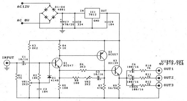
The video amplifier circuit has a maximum gain ratio of only 4 times the impedance is 75 ohms on the input and output, and wide bandwidth of this circuit is 5 Mhz
adjust VR1
1. Adjusting VR1 until the voltage at the base of Q1 is equal to one volt. And is the voltage drop across R7. (No input signal). Approximately 0.75 volts.
2. Adjust VR1 in the middle Enter the input signal is 1 Vp-p, then adjust VR2 to have the lowest rate of increase.
Then turn on the TV or monitor to the output and then adjust VR1 until the test signal to be applied without distortion.
PCB

Saturday, October 18, 2014
Windshield Washer Control Automatic Diagram Circuit
Unfortunately, many ‘low end’ cars or some of the older cars are not equipped with this automatic function which is a very nice convenience to have. So, since all that is required is a handful of components that any electronics hobbyist worthy of the name already has in his/her drawer, we will discuss the circuit proposed here. This project is super simple and simply keeps the windshield wiper activated for a few seconds after the windshield washer control contact has been released.
While the windshield washer pump is operating, the 12 volts delivered by the battery are present at the terminals and are therefore charging capacitor C1. Once the windshield washer has stopped, this capacitor can only discharge through R2, P1, R3, and the T1 emitter-base junction, due to the presence of diode D1. It thus keeps T1 in the conductive state during a certain time, the exact period of which depends on the setting of P1. T1 in turn saturates T2, which then does the same for T3.
Circuit diagram:
The Re1 relay is therefore connected which maintains the windshield wiper in operation because its work contact is wired in parallel to the control switch. Once C1 is sufficiently discharged, T1 is blocked, which then blocks T2 and T3 and deactivates relay Re1. The type of components is not really critical, even if we indicate specific reference numbers for T3, any low-power npn transistor with a gain over 25 will work. However, considering the amount of power consumed by the windshield wiper motor, relay Re1 will imperatively be an ‘automobile’ relay.
You can find very low-priced ones at many car accessory shops (and even at some component retailers). These relays maintain contact under 12 volts and often do not have more than one work contact but they are, in general, capable of cutting off about 20 amps. Finally, the only delicate point of this project is to properly identify the control wire for the windshield pump on one hand, and the windshield wiper motor on the other. Observing what is happening at the various connections with a simple voltmeter, should get it right without too much difficulty.
Copyright: Elektor Electronics
Monday, October 13, 2014
2003 Suzuki DL1000 Radiator Schematic Diagram and Parts Components
Radiators are heat exchangers used to transfer thermal energy from one medium to another for the purpose of cooling and heating. The following schematic diagram shows detail of 2003 Suzuki DL1000 Radiator and its Parts Components which consist of 1. radiator assembly, 2. fan assembly, 3. cushion, 4. cushion, 5. spacer, 6. bolt (6×20), 7. shield, radiator heat, 8. bolt. 9. nut.
Thursday, October 2, 2014
Voltage and Frequency Calibrator Circuit Using IC 555
The 555 timer IC is used in a slightly unusual configuration, having the advantage that an exact 50:50 mark/space ratio may be attained by trimming R1. The frequency of oscillation may be set between l0 kHz and 1 kHz by switching timing capacitors C14. C5 decouples the internal ref- erence potential-divider of the 555 from supply·transients. The squarewave output from pin 3 of the IC, while stable in frequency, is not stable in peak-to-peak voltage as this depends on the supply voltage. This is used to switch on and off a temperature compensated constant- current source O1. R2 ensures that the current·source turns off completely when pin 3 goes high. The current- source output, trimmed by R3 to be exactly 1 mA, drives a resistor ladder network so that a series of precise squarewave voltages are generated. The advantage of current drive rather than voltage drive for this sort of net- work is that calibration is much easier. A simple ladder network is shown by way of example, and more complex ones may simply be constructed to give a wider variety of output voltages. The non-standard component values used were obtained by paralleling standard values. For the timing capacitors several in parallel had to be used, and only the resultant value is shown on the diagram.

Friday, September 26, 2014
How to Design and Make Transformer at Home
This will help electronic hobbyists to design and construct their own transformers according to their needs. In the following pages, a simplified design procedure is given so as to obtain satisfactorily designed transformers. However, the design procedure is often a matter of trial and error.
The tables provided here cut calculations short and help the designer to choose the proper size of wire or core lamination. Only relevant data and calculations are provided so that the designer is not confused by unnecessary details.
The transformer
A transformer has two or more windings of insulated copper wire over an iron core. They are: one primary winding and one or more secondary windings. Each winding is electrically isolated from the other, but they are magnetically coupled with the help of a laminated iron core. Small transforrners have a shell type construction, i.e. the windings are surrounded by the core as shown in Fig. 1. The power delivered by the secondary is actually transferred from the primary, but at a voltage level determined by the turns ratio of the two windings.
Making the Preliminary Transformer design
As the first step to the design of a transformer, the primary and secondary voltage ratings and the secondary current rating must be clearly stated. Then decide on the core material to be used: ordinary steel stampings or cold rolled grain oriented (CRGO) stampings. CRGO has a higher allowable flux density and lower losses.
Core area = 1.l52 x root of (Output voltage x output current) sq. cm.
For transformers with multiple secondaries, the sum of the output volt-amp. product of each winding is to be used. The number of tums on the primary and secondary windings is decided by the turns per volt ratio as:
Turns per volt = 1/ (4.44 X l0^-4 frequency x core area x flux density)
Here, the frequency is 50Hz for Indian domestic mains supply. The flux density can be taken as about 1.0 Weber/ sq. m. for ordinary steel stampings and about 1.3 Weber/ sq. m. for CRGO stampings.
Primary winding design
The current in the primary winding is given by:
Primary Current = Sum of (output volts x output amps)/(Primary volts x efficiency)
The efficiency of small transformers varies between 0.8 to 0.96. A value of 0.87 can be used for ordinary transformers. The proper wire size has to be selected for the winding. The wire diameter depends on the current to be supplied by the winding and the allowable current density of the wire. The current density may be as high as 233 amps/ sq. cm. in small transformers and as low as 155 amps/sq. cm. in large ones. Usually, a value of 200 amps/ sq. cm. can be taken, on whose basis Table 1 is given.
The number of tums in the primary winding is given by:
Primary turns = Turns per volt x primary volts.
The space taken up by the winding will depend on the insulation thickness, method of winding and the wire diameter. Table I gives the approximate values of the turns per square cm. from which we can estimate the window area occupied by the primary winding.
Primary Winding Area = Primary turns/Turns per sq. cm. from Table1
Secondary winding design
Since we have assumed that we know the secondary current rating, we can find out the wire size for the secondary winding by referring to Table 1 directly.
The number of turns on the secondary is calculated in the same way as for the primary, but about 3% extra turns are to be added to compensate for the internal drop of secondary voltage of the transformer, upon loading. Thus,
Secondary Turns = 1.03 (turns per volt x secondary volts)
The window area required for secondary winding is found from Table1 as
Secondary window area = Secondary Turns/Turns per sq. cm from Table1

Core size
The main criterion in selecting the core is the total window area of winding space available.
Total window area = Primary window area + sum of secondary window areas + space for former and insulation
Some extra area is required to accommodate the former and insulation between windings. The actual amount of extra area varies, although 30% may be taken to start with but may have to be modified later. The suitable core sizes having a larger window area are selected from Table ll. . Taking into account the gap between laminations while stacking them (the core stacking factor taken as 0.9), we have
Gross core area = Core Area/0.9 sq.cm.
ln general, a square central limb is preferred. For this, the width of the tongue of lamination is
Tongue width = root of Gross core area cm.
Now refer to Table ll again and finally select the proper i core size, with sufficient window area and a close value of the tongue width as calculated. Adjust the stack height as required to obtain the required core section.
Stack height = Gros core area/Actual tongue width cm.
The stack should not be much less than the tongue width but may be more. However, it should not be more than 1% times the tongue width.

How to Design and Make a Transformer finally
The windings are wound on an insulating former which .fits over the center limb of the core.The primary is usually wound first, then the secondary, with insulation between windings, A final insulating layer is provided over the windings to protect them from mechanical damage. When thin wires are used, their ends must be soldered to thicker wires for bringing the terminals outside the former. The laminations are assembled over the former with alternate laminations reversed in assembly. The laminations must be held together tightly by a suitable clamping frame or by screws (if holes are provided in the laminations).

Shield
lt is a good practice to use an electrostatic shield between the primary and secondary windings to prevent disturbances from passing through to the secondary from the primary. The shield is made out of a copper foil which is wound between the two windings for slightly over a tum. Insulation must be provided along the length of the foil and care taken so that the- two ends of the foil do not touch each other. A wire soldered to the foil is bought out and connected to the ground.

A practical design example can be witnessed below:

Tuesday, September 23, 2014
Guitar Amplifier circuit and explanation
10W Old-Style ultra-compact Combo, Two inputs – Overdrive – Treble-enhancement
The aim of this design was to reproduce a Combo amplifier of the type very common in the ‘sixties and the ‘seventies of the past century. It is well suited as a guitar amplifier but it will do a good job with any kind of electronic musical instrument or microphone. 5W power output was a common feature of these widespread devices due to the general adoption of a class A single-tube output stage (see the Vox AC-4 model). Furthermore, nowadays we can do without the old-fashioned Vib-Trem feature frequently included in those designs. The present circuit can deliver 10W of output power when driving an 8 Ohm load, or about 18W @ 4 Ohm. It also features a two-FET preamplifier, two inputs with different sensitivity, a treble-cut control and an optional switch allowing overdrive or powerful treble-enhancement.
Circuit diagram:
Parts:
P1______________4K7 Linear Potentiometer
P2_____________10K Log. Potentiometer
R1,R2__________68K 1/4W Resistors
R3____________220K 1/4W Resistor
R4,R6,R11_______4K7 1/4W Resistors
R5_____________27K 1/4W Resistor
R7______________1K 1/4W Resistor
R8______________3K3 1/2W Resistor
R9______________2K 1/2W Trimmer Cermet
R10___________470R 1/4W Resistor
R12_____________1K5 1/4W Resistor
R13___________470K 1/4W Resistor
R14____________33K 1/4W Resistor
C1____________100pF 63V Ceramic Capacitor
C2____________100nF 63V Polyester Capacitor
C3____________470µF 35V Electrolytic Capacitor
C4____________220nF 63V Polyester Capacitor (Optional, see Notes)
C5_____________47µF 25V Electrolytic Capacitor (Optional, see Notes)
C6______________1µF 63V Polyester Capacitor
C7,C8,C9,C10___47µF 25V Electrolytic Capacitors
C11____________47pF 63V Ceramic Capacitor
C12__________1000µF 35V Electrolytic Capacitor
C13__________2200µF 35V Electrolytic Capacitor
D1_____________5mm. Red LED
D2,D3________1N4004 400V 1A Diodes
Q1,Q2________2N3819 General-purpose N-Channel FETs
Q3____________BC182 50V 200mA NPN Transistor
Q4____________BD135 45V 1.5A NPN Transistor (See Notes)
Q5____________BDX53A 60V 8A NPN Darlington Transistor
Q6____________BDX54A 60V 8A PNP Darlington Transistor
J1,J2________6.3mm. Mono Jack sockets
SW1____________1 pole 3 ways rotary switch (Optional, see Notes)
SW2____________SPST Mains switch
F1_____________1.6A Fuse with socket
T1_____________220V Primary, 48V Center-tapped Secondary 20 to 30VA Mains transformer
PL1____________Male Mains plug
SPKR___________One or more speakers wired in series or in parallel, Total resulting impedance: 8 or 4 Ohm, Minimum power handling: 20W
| Elektor 303 Circuit |
| Practical Arduino |
| Elektor05-2010 |
| Elektor05-2010 |
| Elektor05-2010 |
| Nuts Volts 06-2010 |
| Nuts Volts 06-2010 |
source:http://electronicsprojects.mediadir.in/guitar-amplifier/
Notes:
- SW1 and related capacitors C4 & C5 are optional.
- When SW1 slider is connected to C5 the overdrive feature is enabled.
- When SW1 slider is connected to C4 the treble-enhancer is enabled.
- C4 value can be varied from 100nF to 470nF to suit your treble-enhancement preferences.
- In all cases where Darlington transistors are used as the output devices it is essential that the sensing transistor (Q4) should be in as close thermal contact with the output transistors as possible. Therefore a TO126-case transistor type was chosen for easy bolting on the heatsink, very close to the output pair.
- To set quiescent current, remove temporarily the Fuse F1 and insert the probes of an Avo-meter in the two leads of the fuse holder.
- Set the volume control to the minimum and Trimmer R9 to its minimum resistance.
- Power-on the circuit and adjust R9 to read a current drawing of about 25 to 30mA.
- Wait about 15 minutes, watch if the current is varying and readjust if necessary.
Technical data are quite impressive for so simple a design:
Sensitivity:
30mV input for 10W output
Frequency response:
40 to 20KHz -1dB
Total harmonic distortion @ 1KHz and 10KHz, 8 Ohm load:
below 0.05% @ 1W, 0.08% @ 3.5W, 0.15% at the onset of clipping (about 10W).
Monday, September 22, 2014
500W low cost 12V to 220V inverter circuit and explanation
Using this circuit you can convert the 12V dc in to the 220V Ac. In this circuit 4047 is use to generate the square wave of 50hz and amplify the current and then amplify the voltage by using the step transformer.
author: Ashad Mustufa
e-mail: mustufa66@hotmail.com
web site: http://www.electronics-lab.com
Circuit diagram

How to calculate transformer rating
The basic formula is P=VI and between input output of the transformer we have Power input = Power output
For example if we want a 220W output at 220V then we need 1A at the output. Then at the input we must have at least 18.3V at 12V because: 12V*18.3 = 220v*1
So you have to wind the step up transformer 12v to 220v but input winding must be capable to bear 20A.
0 50V 2A Bench power supply circuit and description
Circuit diagram
I use the lm10 IC because it has a reference voltage and that’s useful for dc power supply. With two ICs can take different output voltage and amperage. This circuit is protected from short circuit.P2 is for controlling the current at the range of 0-2A. Stabilize the output voltage with R4 on negative pin on op-amp and with R2 & P1 on positive pin.
Op-amp output controls T1 that not let ripple of voltage.T1 increase or decrease ampere of R6 and control the voltage of T5 & T4. Pin 1 is the reference voltage and reference voltage is losing some voltage on R1 that has 100uA . This current passes through P1 too.
Vlose p1=100uA*Rp1
This lose voltage regulate output voltage rate of output current is compare between reference voltage of P3 and lose voltage on R11.T3 is protecting short circuit with R11. For reduce out put voltage to 0v should parallel one resistor 470 ohm in out put. Minimum voltage is 0.4v. The maximum output voltage is fixed with R1b and should not become over of 50v. Therefore your transformer should give 36V, 3A with 4700uF capacitor. T6, T5, T7 need heatsilk.
R1a = 2,2 K
R1b = read the text
R2 = 10 K
R3, R7 = 3.3 k
R4 = 390 Ohm
R5 = 47 K
R6 = 3.3 K 1Watt
R8 = 180 Ohm
R9, R10 = 0.47 Ohm 3Watt
R11 = 0.075 Ohm 2Watt
R12 = 470 Ohm
P1 = 500K liner potentiometer
P2 = 4.7 K potentiometer
P3 = 10 K potentiometer
C1 = 1nF
C2 = 10nF
C3 = 22nF
C4 = 47mF 63v electrolytic
C5 = 4700mF 80v electrolytic
T1, T2 = BC161
T3, T4 = BD141
T5 = BD241
T6, T7 = 2V3055
D1, D2 = 1N4148
D3, D4 = 1N4001
IC1, IC2 = LM10C
author:
e-mail: hamed_iranmehr@yahoo.com
web site: http://www.electronics-lab.com
0 50V 2A Bench power supply circuit and explanation
I use the lm10 IC because it has a reference voltage and that’s useful for dc power supply. With two ICs can take different output voltage and amperage. This circuit is protected from short circuit.P2 is for controlling the current at the range of 0-2A. Stabilize the output voltage with R4 on negative pin on op-amp and with R2 & P1 on positive pin.
Op-amp output controls T1 that not let ripple of voltage.T1 increase or decrease ampere of R6 and control the voltage of T5 & T4. Pin 1 is the reference voltage and reference voltage is losing some voltage on R1 that has 100uA . This current passes through P1 too.
Vlose p1=100uA*Rp1
This lose voltage regulate output voltage rate of output current is compare between reference voltage of P3 and lose voltage on R11.T3 is protecting short circuit with R11. For reduce out put voltage to 0v should parallel one resistor 470 ohm in out put. Minimum voltage is 0.4v. The maximum output voltage is fixed with R1b and should not become over of 50v. Therefore your transformer should give 36V, 3A with 4700uF capacitor. T6, T5, T7 need heatsilk.
R1a = 2,2 K
R1b = read the text
R2 = 10 K
R3, R7 = 3.3 k
R4 = 390 Ohm
R5 = 47 K
R6 = 3.3 K 1Watt
R8 = 180 Ohm
R9, R10 = 0.47 Ohm 3Watt
R11 = 0.075 Ohm 2Watt
R12 = 470 Ohm
P1 = 500K liner potentiometer
P2 = 4.7 K potentiometer
P3 = 10 K potentiometer
C1 = 1nF
C2 = 10nF
C3 = 22nF
C4 = 47mF 63v electrolytic
C5 = 4700mF 80v electrolytic
T1, T2 = BC161
T3, T4 = BD141
T5 = BD241
T6, T7 = 2V3055
D1, D2 = 1N4148
D3, D4 = 1N4001
IC1, IC2 = LM10C
author:
e-mail: hamed_iranmehr@yahoo.com
web site: http://www.electronics-lab.com
Thursday, September 18, 2014
Circuit Cat And Dog Repellent
This frequency is above the hearing threshold for humans but is known to be irritating frequency for dog and cats. Since the maximum current that a 555 timer can supply is 200mA an amplifier stage was required so a high-power H-bridge network was devised, formed by 4 transistors TR1 to TR4. A second timer IC2 forms a buffer amplifier that feeds one input of the H-bridge driver, with an inverted waveform to that of IC1 output being fed to the opposite input of the H-bridge.
Circuit diagram:

This means that conduction occurs through the complementary pairs of TR1/TR4 and TR2/TR3 on alternate marks and spaces, effectively doubling the voltage across the ultrasonic transducer, LS1. This is optimised to generate a high output at ultrasonic frequencies. This configuration was tested by decreasing the frequency of the oscillator to an audible level and replacing the ultrasonic transducer with a loudspeaker; the results were astounding. If the dog repellent circuit was fed by a bench power supply rather than a battery that restrict the available current, the output reached 110dB with 4A running through the speaker which is plenty loud enough!
The Dog and Cat repellant was activated using a normal open switch S1 to control the current consumption, but many forms of automatic switching could be used such as pressure sensitive mats, light beams or PIR sensors. Thus it could be utilise as part of a dog or cat deterrent system to help prevent unwanted damage to gardens or flowerbeds, or a battery powered version can be carried for portable use. Consider also using a lead-acid battery if desired, and a single chip version could be built using the 556 dual timer IC to save space and improve battery life.
Sunday, September 14, 2014
Classical audio power amplifier with IT and OT transformer

Troubleshooting :
Wether transistors placement is correct ?
Placement Elco ?
Check are cable .
If all components have benn checked , and the damaged has been replaced . Then try , turn the potentiometer slowly and listen to how the sound output by the speaker.
Saturday, September 13, 2014
Power amplifier with load detection and auto BTL SE selection
 |
| Power amplifier with load detection and auto BTL/SE selection |
Part 4 Contact info and web adresses of integrated circuits power audio amplifiers manufacturers

Mag- Magnatec (Semelab Subdivision)
Semelab Plc. Coventry Road, Lutterworth, UK. Phone: +44-1455-552505
http://www..semelab.co.uk
Max- Maxim Integrated Products
120 San Gabrial Sunnyvale, CA 94086, USA. Phone: +1-800-998-8800
http://www.maxim-ic.com
Mcp- Microchip Technology Inc.
2355 West Chandler Blvd. Chandler, AZ 85224-6199, USA. Phone: 480-792-7200
http://www.microchip.com
Mit- Mitsubishi Electric Co. Ltd. (ICs manufacture is handed to Renssas Ltd.)
2-3 Marunouchi, 2-chome J 100 Chiyoda-Ku, Tokyo, Japan. Phone: +81-3-3218-2863
http://www.mitsubishichips.com
Mot- Motorola Inc. (ICs manufacture is handed to ON Semiconductor)
6501 William Cannon Drive W Austin, TX 78735 USA. Phone: +1-512-891-2000
http://www.motorola.com
Mps- Monolithic Power Systems
6409 Guadalupe Mines Road, San Jose, CA 95120, USA. Phone: 408-826-0600
http://www.monolithicpower.com
Mts- Mitsumi Electric Co. Ltd.
8-8-2, Kokuryo-cho, Chofu-chi, Tokyo 182-8557, Japan. Phone: (03)3489-5333
http://www.mitsumi.co.jp
Msk- M.S.Kennedy Corp.
4707 Dey Road Liverpool, N.Y. 13088 USA . Phone (315) 701-6751
www.mskennedy.com
Mul- Mullard LTD (Is not a current ICs manufacturer)
New Road Mitcham, Surrey England CR4 4XY. Telex: 264341
NEC Electronics Inc. (Nippon Electrical Company)
NEC Building 7-1, Shiba 5-chome, Minato-ku Tokyo, Japan. Phone: +81-3-3454-1111
http://www.ic.nec.co.jp
NJR- New Japan Radio Co., Ltd.
Arvco Tower 17F, 1-8-1, Shimomeguro, Meguro-ku, Tokyo 153, Japan.
Phone: +81-3-5434-8335
http://www.njr.com
Npc- Nippon Precision Circuits Inc.
4-3, Fukuzumi 2-chome, Koto-ku, Tokyo 135-8430, Japan. Phone:+81-3-3642-6661
http://www.npc.co.jp/453
NSC- National Semiconductor Corp.
North America PO Box 7643 Mount Prospect, IL 60056-7643, USA.
Phone: +1-800-628-7364, ext 305
http://www.national.com
NTE Electronics Inc.
44 Farrand Street, Bloomfield, NJ 07003, USA. Phone: 800-631-1250
http://www.nteinc.com
Nxp- NXP Semiconductors
PO Box 80073, 5600 KA Eindhoven, Netherlands. Phone: +31 40 27 45678
http://www.nxp.com
Oki Semiconductor Inc.
785 N Mary Avenue Sunnyvale, CA 94086, USA .Phone: +1-408-720-1900
http://www.okisemi.com
Omn- Omnirel (Acquired by International Rectifier)
205 Crawford Street, Leominster, MA 01453 USA. Phone: (508) 534-5776
http://www.omnirel.com
Ons- ON Semiconductor (Motorola semiconductors subdivision)
Japan Customer Focus Center 4321 NishiGotanda, Shinagawaku, Tokyo, Japan
Phone: 81357402745
http://onsemi.com
Pan- Panasonic Electronics Corp.
1 Kotari-Yakemashi, Nagaokakyo, Kyoto 617, Japan. Phone: 075/921-8151
http://www.mec.panasonic.co.jp
Pch- PointChips Co. Ltd.
4FL., Dabong Tower Bldg. 890-12, Daechi-Dong, Kangnam-Gu, Seoul 135-280, Korea
Phone: 82-2-508-2443
http://www.pointchips.com
Phi- Philips GmbH (ICs manufacture is handed to NXP Semconductor)
Hammerbrookstrasszlige 69 D-20097 Hamburg, Germany. Phone: +49-40-23536-0
http://www.philips.com
Pjn- Promax-Johnton
(There is no accesible padding information)
http://www.p-johnton.com
Pls- GEC Plessey Semiconductor
(Is not a current ICs manufacturer)
Pnr- Pioneer Not the manufacturer of ICs
Will use custom IC with Pioneer type marking
Ptc- Princeton Technology Corp.
2F, No. 233-1, Baociao Road, Sindian City, Taipei 23145, Taiwan, R.O.C.
Phone: 886-2-66296288
http://www.princeton.com.tw
Rca- RCA Corporation (Is not a current ICs manufacturer)
Route 202, Sommerville, NJ 08876, USA. Phone: 201/685-6423
http://www.rca.com
Ren- Renessas Ltd.
Nippon Bldg., 2-6-2, Ohte-machi, Chiyoda-ku, Tokyo 100-0004, Japan,
Phone: 852-2424-9127
http://www.renesas.com
Tuesday, September 9, 2014
LM2575 and LM2577 Regulator Switching Circuit
Via:[http://www.diagramtoday.com/switching-regulators-using-lm-2575-and-lm-2577]
