Showing posts with label converter. Show all posts

Thursday, November 13, 2014

ADV7123 Digital to Analog Converter Connection Diagram and Datasheet


This digital-to-analog converter (DAC) integrated circuit is designed for lowest noise performance, both radiated and conducted noise. A recommended connection diagram for the ADV7123 is shown in the following schematic diagram.

According to the ADV7123 datasheet, this device consists of three high speed, 10-bit, video DACs with complementary outputs, a standard TTL input interface, and a high impedance, analog output current source. It used to be applied in digital video systems, image processing, digital radio modulation, color graphics and more.

Additional information on ADV7123 Digital-to-Analog Converter Connection Diagram can be seen in this datasheet of pdf filetype (source: analog.com).

Read More..

Tuesday, November 4, 2014

VGA to TV Converter Circuit

VGA to TV Converter Circuit

This converter circuit basically takes VGA signals and converts it to RGB + composite sync signal which can be fed to TV via SCART connector. VGA card picture components RED, GREEN and BLUE are already at the correct voltage level (0.7Vpp) and has correct impedance (75 ohm) for direct connection to correspondign inputs in the TV.
VGA to TV Converter Ciruit


VGA to TV Converter Printed Circuit Board (PCB)


For combining separate horizonal and vertical sync signal from VGA card to one composite sync signal needs a sync signal conversion which is feed to TV video in pin in SCART connector. The tv converter circuit has also sends correct level signal to the TV RGB input enabling control pin in the SCART connector (pin 16).
The circuit is simply based on one TTL chip with four XOR ports, two resistors and two capacitors. TTL chip was logical choise because VGA sync signals are TTL level signals.

The sync signal combiner has a system to adjust to different sync polarities so that it always makes correct composite sync signals. VGA card uses different sync signal polarities to tell the monitor which resolution is used. This circuit adjusts to sync signal polarity changes in less than 200 milliseconds, which is faster than setting time of a normal VGA monitor in the display mode change. The tv converter circuit needs well regulates +5V (+/-5%) power supply and takes about 120 mA current.

VGA to TV converter parts list are as follow:

Main circuit

U1 74LS86 (74HC86 or 74HCT86 can also be used)

C1 22 microfarads 16V electrolytic capacitor

C2 use 47 uF 16V electrolytic for more reliable operation (22 uF listed schematic can cause problems in some cases)

R1,R2 2.2 kohm, 1/4 W

R3,R4,R5 2.2 kohm, 1/4 W

R6,R7,R9 47 ohm, 1/2 W

R8 120 ohm, 1/2 W

T1,T2 BC547B (2N2222 should also work but note the different pinout)

P1 15 pin SUB-D connector (DE-15)

Output connector

21 pin EURO/SCART connector

Wiring:

Red, Green, Blue and Composite Sync lines should be wired using 75 ohm coaxial cable for best picture quality, but can be replaced with normal shielded wire.

Power supply components

7805 regulator chip

100 uF electrolytic 25V

10 uF electrolytic 16V

100 nF polyester or ceramic condensator

Wall adapter which outputs 8-18V DC and 150 mA or more current

Connector for connecting wall adaptor to circuit 
Read More..

Thursday, October 23, 2014

12V Step Down Dc Converter Using ADP2300 ADP2301

Using ADP2300 ADP2301 step-down dc dc regulators with integrated power MOSFET, can be designed a very simple DC DC voltage converter. Output voltage delivered by these circuits can be adjusted from 0.8 volts, up to 0.85xVin , with ±2% accuracy. The maximum output current that can be provided by ADP2300 ADP2301 regulators is up to 1.2 A load current.

12V Step-Down Dc Converter Circuit Diagram
12V Step-Down Dc-Converter-Circuit Diagram
12V Step-Down Dc-Converter-ADP2301
There are two frequency options: the ADP2300 runs at 700 kHz, and the ADP2301 runs at 1.4 MHz. These options allow users to make decisions based on the trade-off between efficiency and total solution size. Current-mode control provides fast and stable line and load transient performance.  Bellow you an see two design examples, which require few common electronic components.First circuit will provide a 2.5V output at a maximum current of 1.2A from an input voltage of 12 volts. Second circuit will provide a 5V output at a maximum current of 1.2A from an input voltage of 12 volts.
Read More..

6 to 15 Volt DC Converter

A very efficient 6V to 15V DC to DC converter using LM2585 is publicized at this time. LM2585 is a monolithic integrated voltage converter IC with the intention of can be situated used stylish various applications like flyback converters, boost converters, advance converters, multiple output converters and the rest. The circuit requires lowest possible amount of outdoor components and the IC can source up to 3A output current.
at this juncture the IC is wired for instance a boost converter somewhere resistors R1 and R2 are used to established the output voltage .The junction of R1 and R2 is connected to the comment pin of IC1. Capacitor C4 is the input filter while capacitor C1 the filter on behalf of output. set of contacts comprising of resistor R1 and capacitor C2 is intended for frequency compensation. Inductor L1 provisions the energy for acquiring boost conversion.


6 to 15 Volt DC Converter

Read More..

Monday, October 20, 2014

Build a 12V To 24V DC DC Converter Circuit Diagram

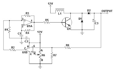
Build a 12V To 24V DC-DC Converter Circuit Diagram.This simple 12V To 24V DC-DC Converter Circuit Diagram can provide up to 24V from a 12V source. It can be used to run radios, small lights, relays, horns and other 24V accessories from a 12V vehicle with a maximum draw of about 800mA. 

It can be used to charge one 12V battery from another, or step up the voltage just enough to provide necessary overhead for a 12V linear regulator. Using one op-amp as a square wave oscillator to ring an inductor and another op-amp in a feedback loop, it wont drift around under varying loads, providing a stable 24V source for many applications. With a wide adjustment in output this circuit has many uses.

 12V To 24V DC-DC Converter Circuit Diagram

12V To 24V DC-DC Converter Circuit Diagram

Parts

Part
Total Qty.
Description
Substitutions
R1, R2, R3, R4, R8, R76100K 1/4W Resistor
R51470 Ohm 1/2W Resistor
R6110K Linear Pot
C110.01uF Mylar Capacitor
C210.1uF Ceramic Disc Capacitor
C31470uF 63V Electrolytic Capacitor
D111N4004 Rectifier Diode
D21BY229-400 Fast Recovery DiodeSee Notes
Q11BC337 NPN Power Transistor
U11LM358 Dual Op Amp IC
L11See Notes
MISC1Board, Wire, Socket For U1, Case, Knob For R6, Heatsink for Q1

Notes

  • R6 sets the output voltage. This can be calculated by Vout = 12 x (R8/(R8+R7)) x (R6B/R6A).
  • L1 is made by winding 60 turns of 0.63MM magnet wire on a toroidial core measuring 15MM (OD) by 8MM (ID) by 6MM (H).
  • D2 can be any fast recovery diode rated at greater then 100V at 5A. It is very important that the diode be fast recovery and not a standard rectifier.
  • Q1 will need a heatsink.


Sourced By Circuitsstream
Read More..

Friday, October 17, 2014

Valve Sound Converter Circuit Diagram

‘Valve sound’ is not just an anachronism: there are those who remain ardent lovers of the quality of sound produced by a valve amplifier. However, not everyone is inclined to splash out on an expensive valve output stage or complete amplifier with a comparatively low power output. Also, for all their aesthetic qualities, modern valve amplifiers burn up (in the full sense of the word!) quite a few watts even at normal listening volume, and so are not exactly environmentally harmless. This valve sound converter offers a cunning way out of this dilemma. It is a low cost unit that can be easily slipped into the audio chain at a suitable point and it only consumes a modest amount of energy.


 Valve Sound Converter Circuit Diagram


A valve sound converter can be constructed using a common-or-garden small-signal amplifier using a readily-available triode. Compared to using a pentode, this simplifies the circuit and, thanks to its less linear characteristic, offers even more valve sound. For stereo use a double triode is ideal. Because only a low gain is required, a type ECC82 (12AU7) is a better choice than alternatives such as the ECC81 (12AT7) or ECC83 (12AX7). This also makes things easier for home brewers only used to working with semiconductors, since we can avoid any difficulties with high voltages, obscure transformers and the like:the amplifier stage uses an anode voltage of only 60 V, which is generated using a small 24 V transformer and a voltage doubler (D3, D4, C4 and C5).

Since the double triode only draws about 2mA at this voltage, a 1 VA or 2 VA transformer will do the job. To avoid ripple on the power supply and hence the generation of hum in the converter, the anode voltage is regulated using Zener diodes D1 and D2, and T1. The same goes for the heater supply: rather than using AC, here we use a DC supply, regulated by IC1. The 9 V transformer needs to be rated at at least 3 VA. As you will see, the actual amplifier circuit is shown only once. Components C1 to C3, R1 to R4, and P1 need to be duplicated for the second channel.


The inset valve symbol in the circuit diagram and the base pinout diagram show how the anode, cathode and grid of the other half of the double triode (V1.B) are connected. Construction should not present any great difficulties. Pay particular attention to screening and cable routing, and to the placing of the transformers to minimise the hum induced by their magnetic fields. Adjust P1 to set the overall gain to 1 (0 dB). The output impedance of 47 kΩ is relatively high, but should be compatible with the inputs of most power amplifiers and preamplifiers.

For a good valve sound, the operating point of the circuit should be set so that the audio output voltage is in the region of a few hundred millivolts up to around 1.5 V. If the valve sound converter is inserted between a preamplifier and the power amplifier, it should be before the volume control potentiometer as otherwise the sound will change significantly depending on the volume. As an example, no modifications are needed to an existing power amplifier if the converter is inserted between the output of a CD player and the input to the amplifier.
Read More..

Sunday, October 5, 2014

2N3055 DC 12V to DC 6V 7 5V 9V Converter


This circuit is DC to DC converter model step down voltage. That can modify voltage input 12V DC from be DC 6V , 7.5V and 9V by have the size current about 1A – 2 Amp think. Be easy circuit use Zener diode maintain one’s position voltage. Be stable and have transistor 2N3055. 
Read More..

Saturday, September 6, 2014

How to Build a 2 to 4 Wire Audio Converter

This audio converter schema maintains 40 dB of isolation between the two halves of entry and exit of a four-line son, while allowing a line connecting two son. A balancing potentiometer, R, adjusts the gain of zero lC2to crossing the inlet to the outlet .

The adjustment is done in terms of work just after installation by inserting a 1 kHz tone at the entrance of four son and setting R to the minimum output signal 82-ohm dummy-load resistor is placed between two wire terminals .

 2 to 4 Wire Audio Converter Circuit Diagram

How

Read More..

Saturday, August 23, 2014

12 Volt to 32 Volt CT converter DC to DC

12Volt
Kit that can change the normal 12v dc voltage from a car battery, battery bike 12V motor. With the current 7A. so this circuit is very suitable for power car amplifiers and sound systems that use simple 12V battery.


Kit converter is also equipped with inputs "SEND" to activate the circuit and also send this interchangeable inputs is connected to the Tape / cd / dvd player of your car. And input "send" is if the non-connected with an output of "send" player car you then connect it to +12 hrs on v from the battery / batteries The series is already in the test kit and has been functioning normally.


Read More..

Tuesday, August 19, 2014

4 Bit Analogue to Digital Converter Wiring diagram Schematic

The operation of the converter is based on the weighted adding and transferring of the analogue input levels and the digital output levels. It consists of comparators and resistors. In theory, the number of bits is unlimited, but each bit needs a comparator and several coupling resistors. The diagram shows a 4-bit version. The value of the resistors must meet the following criteria:
  • R1:R2 = 1:2;
  • R3:R4:R5 = 1:2:4;
  • R6:R7:R8:R9 = 1:2:4:8.
The linearity of the converter depends on the degree of precision of the value of the resistors with respect to the resolution of the converter, and on the accuracy of the threshold voltage of the comparators. This threshold level must be equal, or nearly so, to half the supply voltage. Moreover, the comparators must have as low an output resistance as possible and as high an input resistance with respect to the load resistors as feasible. Any deviation from these requirements affects the linearity of the converter adversely.

4-Bit Analogue to Digital Converter Circuit Diagram

4-Bit
4-Bit Analogue to Digital Converter Circuit Diagram

If the value of the resistors is not too low, the use of inverters with an FET (field-effect transistor) input leads to a near-ideal situation. In the present converter, complementary metal-oxide semiconductor (CMOS) inverters are used, which, in spite of their low gain, give a reasonably good performance. If standard comparators are used, take into account the output voltage range and make sure that the potential at their non-inverting inputs is set to half the supply voltage. If high accuracy is a must, comparators Type TLC3074 or similar should be used. This type has a totem-pole output. The non-inverting inputs should be interlinked and connected to the tap of a a divider consisting of two 10 kΩ resistors across the supply lines. It is essential that the converter is driven by a low-resistance source. If necessary, this can be arranged via a suitable op amp input buffer. The converter draws a current not exceeding 5 mA.
Read More..

Monday, August 11, 2014

Dual Output dc dc Converter Wiring diagram Schematic

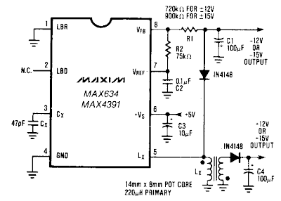
The Dual Output dc-dc Converter Circuit Diagram buck-boost configuration the MAX634 is well suited for dual output dc-dc converters. Only a second winding on the inductor is needed. Typically, this second winding is bifilar-primary and secondary are wound simultaneously using two wires in parallel. 

The inductor core is usually a toroid or a pot core. The negative output voltage is fully regulated by the MAX634. The positive voltage is semi-regulated, and will vary slightly with load changes on either the positive or negative outputs.

Dual Output dc-dc Converter Circuit Diagram

Dual Output dc-dc Converter Circuit Diagram

Read More..

Saturday, August 9, 2014

Sine wave to square wave converter Wiring diagram Schematic

Build a simple Sine wave-to-square wave converter Circuit Diagram. Many signals are digitally generated or transmitted as square waves. It is often desirable to convert these signals into sine. In this Sine wave-to-square wave converter Circuit Diagram The sine input is ac coupled by capacitor C; Rl and R2 bias the input midway between Vn and Vp, the input threshold voltages to provide a square wave at the output. 

 Sine wave-to-square wave converter Circuit Diagram


Sine wave-to-square wave converter Circuit Diagram
Read More..