Showing posts with label low. Show all posts

Sunday, November 9, 2014

Automatic Low Power Emergancy Light

Here is a white-LED-based emergency light that offers the following advantages. 1-It is highly bright due to the use of white LEDs. 2-The light turns on automatically when mains supply fails, and turns off when mains power resumes. 3-It has its own battery charger. When the battery is fully charged, charging stops automatically. The charger power supply section is built around 3-terminal adjustable regulator IC LM317 (IC1), while the LED driver section is built around transistor BD140 (Q2).

In the charger power supply section, an input AC main is stepped down by T1 to deliver 9V, 500mA to the bridge rectifier, which comprises diodes D1 through D4. Filter capacitor C1 eliminates ripples. Unregulated DC voltage is fed to input pin 3 of IC1 and provides charging current through D5 and limiting resistor R15. By adjusting preset P1, the output voltage can be adjusted to deliver the required charging current. When the battery gets charged to 6.8V, D6 conducts and charging current from IC1 finds a path throughQT1 to ground and it stops charging of the battery. When mains power is available, the base of Q2 remains high and Q2 does not conduct. Thus LEDs are off.

On the other hand, when mains fails, the base of Q2 becomes low and it conducts. This makes all the LEDs glow. The mains power supply, when available, charges the battery and keeps the LEDs off as Q2 remains cut-off. During mains failure, the charging section stops working and the B1 supply makes the LEDs glow. Assemble the circuit on a general-purpose PCB and enclose in a cabinet with enough space for battery and switches. We have tested the circuit with twelve 10mm white LEDs. You can use more LEDs provided the total current consumption does not exceed 1.5A. Driver transistor Q2 can deliver up to 1.5A with proper heat-sink arrangement.

Circuit diagram:

Fully Automatic Emergency Light Circuit Diagram
Parts:

P1 = 2.2K
R1-R12 = 100R-1/2W
R13 = 1K-1/2W
R14 = 180R-1/2W
R15 = 16R/5W
R16 = 1.2K
C1 = 1000uF-25V
D1-D5 = 1N4007
D6 = 6.8V-0.5W Zener
D7-D18 = 10mm- White LEDs
Q1 = BC548
Q2 = BD140
B1 = 6V-4.5Ah Battery
IC1 = LM317
T1 = 9Vac-Transformer
Read More..

Saturday, November 8, 2014

Low Cost Universal Battery Charger Schematic

Here is the circuit diagram of a low cost universal charger for NiCD - NiMH batteries. This circuit is Ideal for car use. It has ability to transform a mains adapter in to a charger . This one can be used to charge cellular phone, toys, portables, video batteries, MP3 players, ... and has selectable charge current. An LED is located in circuit to indicate charging. Can be built on a general purpose PCB or a veroboard. I hope you really like it.
Picture of the circuit: 
 A Low Cost Universal Charger Circuit Schematic
Circuit diagram:
A Low Cost Universal Charger Circuit Diagram
Parts:
R1 = 120R-0...5W
R2 = See Diagram
C1 = 220uF-35V
D1 = 1N4007
D2 = 3mm. LED
Q1 = BD135
J1 = DC Input Socket
Specifications:
  • Ideal for in car use.
  • LED charge indication.
  • Selectable charge current.
  • Charges Ni Cd or NiMH batteries.
  • Transforms a mains adapter into a charger.
  • Charge cellular phone, toys, portables, video batteries …
Features:
  • LED function indication.
  • Power supply polarity protected.
  • Supply current: same as charge current.
  • Supply voltage: from 6.5VDC to 21VDC (depending on used battery)
  • Charge current (±20%): 50mA, 100mA, 200mA, 300mA, 400mA. (selectable)
Determining the supply voltage:
This table indicates the minimum and maximum voltages to supply the charger. See supply voltage selection chart below.
Example:
To charge a 6V battery a minimum supply voltage of 12V is needed, the maximum voltage is then 15V.
Voltage selection:

Voltage Selection Chart For Low Cost Universal Battery Charger

Determining the charge current:
Before building the circuit, you must determinate how much current will be used to charge the battery or battery pack. It is advisable to charge the battery with a current that is 10 times smaller then the battery capacity, and to charge it for about 15 hours. If you double the charge current , then you can charge the battery in half the time. Charge current selection chart is located in diagram.

Example:
A battery pack of 6V / 1000mAh can be charged with 100mA during 15 hours. If you want to charge faster, then a charge current of 200mA can be used for about 7 hours.
Caution:
The higher charge current, the more critical the charge time must be checked. When faster charging is used, it is advisable to discharge the battery completely before charging. Using a charge current of 1/10 of the capacity will expand the lifetime of the battery. The charge time can easily be doubled without damaging the battery.
Note:
  • Mount the transistor together with the heatsink on the PCB, bend the leads as necessary. Take care that the metal back of the transistor touches the heatsink. Check that the leads of the transistor do not touch the heatsink. 
Read More..

Thursday, November 6, 2014

Low Cost Power Buzzer

How often on average do you have to call members of your family each day to tell them that dinner is ready, it’s time to leave, and the like? The person you want is usually in a different room, such as the hobby room or bedroom. A powerful buzzer in the room, combined with a push button at the bottom of the stairs or in the kitchen, could be very handy in such situations.

 The heart of this circuit is formed by IC1, a TDA2030. This IC has built-in thermal protection, so it’s not likely to quickly give up the ghost. R1 and R2 apply a voltage equal to half the supply voltage to the plus input of the opamp. R3 provides positive feedback. Finally, the combination of C2, R4 and trimmer P12 determines the oscillation frequency of the circuit.

Power Buzzer Circuit Diagram:
 power buzzer circuit diagram

The frequency of the tone can also be adjusted using P1. There is no volume control, since you always want to get attention when you press pushbutton S1. Fit the entire circuit where you want to have the pushbutton. The loudspeaker can then be placed in a strategic location, such as in the bedroom or wherever is appropriate. Use speaker cable to connect the loudspeaker. Normal bell wire can cause a significant power loss if the loudspeaker is relatively far away. The loudspeaker must be able to handle a continuous power of at least 6 W (with a 20-V supply voltage).

The power quickly drops as the supply voltage decreases (P = Urms 2 / RL). The power supply for this circuit is not particularly critical. However, it must be able to provide sufficient current. A good nominal value is around 400 mA at 20 V. At 4 V, it will be approximately 25 mA. Most likely, you can find a suitable power supply somewhere in your hobby room. Otherwise, you can certainly find a low-cost power supply design in our circuits archive that will fill the bill!

Read More..

Tuesday, October 28, 2014

VHF UHF Low Noise amplifiers MAX2664 MAX2665 circuit

A very simple low cost and ultra compact VHF UHF Low-Noise amplifiers circuit can be designed using the MAX2664 and MAX2665 ultra-compact LNAs for VHF/UHF applications.
These devices incorporate a broadband LNA with an integrated bypass switch. The MAX2664 covers the UHF frequency range from 470MHz to 860MHz, and the MAX2665 covers the VHF frequency range from 75MHz to 230MHz. Each device has a zero-power bypass mode for improved high-signal-level handling conditions.
 As you can see in the presented circuit diagram , this RF project requires very few external components . Both ICs has a high gain around 15dB and require a single power supply , that can provide an output voltage between 2.4 to 3.5 volts .
VHF UHF Low-Noise amplifiers has a very low current consumption of 3.3 mA and can be used in applications like : Smartphones/Handsets , MP3 Players , Home Audio/Video and other portable navigation devices .
Read More..

Minimal low supply rail detection

At this point’s a minimal low supply rail detection circuit with the purpose of expenditure peanuts and takes a short time ago 20 minutes or else so to become. Its power consumption is quite low, so it may perhaps definitely survive built into battery-powered campaign. as an alternative of using an op amp, the circuit is built around three low-cost transistors (Q1-Q3). Diodes D1-D3 form a 1.8V voltage reference (Vref) used for the emitter of Q1. If the voltage across the voltage wall formed by R1 and VR1 is a reduced amount of than this, Q1 turns on and food Q2 with foundation bias current.

Rail

This turns on Q3 here proportion to this bias current which subsequently drives LED1. The brightness of the LED gives an indication of the severity of the low voltage condition. The brighter the LED, the minor the supply voltage. Trimpot VR1 is adjusted so to facilitate LED1 really comes on by the desired low-voltage promontory. The current consumption is typically take away than 2mA at what time LED1 is rotten. in conclusion, the price exposed in support of RLED is right for 6-12V surgery. For other voltages, RLED can ensue calculated using the formula RLED = (Vcc - 1.8)/0.01 (this equates to a current of with reference to 10mA).
Read More..

Wednesday, October 22, 2014

Ultra Low Drop Linear Regulator

The circuit is a MOSFET based linear voltage regulator with a voltage drop of as low as 60 mV at 1 ampere. Drop of a fewer millivolts is possible with better MOSFETs having lower  RDS(on)  resistance. 

The circuit in Fig.1 uses 15V-0-15V secondary output from a step-down transformer and employs an n-channel MOSFET IRF540 to get the regulated 12V output from DC input, which could be as low as 12.06V. The gate drive voltage required for the MOSFET is generated using a voltage doubler circuit consisting of diodes D1 and D2 and capacitors C1 and C4. To turn the MOSFET fully on, the gate terminal should be around 10V above the source terminal which is connected to the output here. The voltage doubler feeds this voltage to the gate through resistor R1. Adjustable shunt regulator TL431 (IC2) is used here as an error amplifier, and it dynamically adjusts the gate voltage to maintain the regulation at the output.
Ultra Low Drop Linear Regulator Circuit Fig-1 Circuit Fig.1

With adequate heatsink for the MOSFET, the circuit can provide up to 3A output at slightly elevated minimum voltage drop. Trimpot VR1 in the circuit is used for fine adjustment of the output voltage. Combination of capacitor C5 and resistor R2 provides error-amplifier compensation. 

The circuit is provided with a short-circuit crow-bar protection to guard the components against over stress during accidental short at the output. This crow-bar protection will work as follows: Under normal working conditions, the voltage across capacitor C3 will be 6.3V and diode D5 will be in the off state since it will be reverse-biased with the output voltage of 12V. However, during output short-circuit condition, the output will momentarily drop, causing D5 to conduct and the opto-triac MOC3011 (IC1) will get triggered, pulling down the gate voltage to ground, and thus limiting the output current. The circuit will remain latched in this state, and input voltage has to be switched off to reset the circuit. 

Ultra Low Drop Linear Regulator fig-2 Circuit Fig.2

The circuit shown in Fig.2 follows a similar scheme. It can be utilised when the regulator has to work from a DC rail in place of 15V-0-15V AC supply. The gate voltage here is generated using an LM555 charge pump circuit as follows: 

When 555 output is low, capacitor C2 will get charged through diode D1 to the input voltage. In the next half cycle, when the 555 output goes high, capacitor C3 will get charged to almost double the input voltage. The rest of the circuit works in a similar fashion as the circuit of Fig. 1. 

The above circuits will help reduce power-loss by allowing to keep input voltage range to the regulator low during initial design or even in existing circuits. This will keep the output regulated with relatively low input voltage compared to the conventional regulators. 

The minimum voltage drop can be further reduced using low RDS(on) MOSFETs or by paralleling them.


Source by : Ecircuitslab
Read More..

Sunday, October 5, 2014

5V Regulator Ultra Low Power Circuit


5V Regulator Ultra Low-Power Circuit by http://www.extremecircuits.net

The accepted cesspool of the regulator is minute compared with that of, say, a 78L05: at an ascribe voltage of 9 V and open-circuit output, it is aloof beneath 50 µA. The ambit consists of a aboveboard bandgap advertence based on T1 and IC1, followed by an amplifier formed by IC2 and T1. The advertence voltage is about 1.22 V, which is aloft by IC2 to 5 V. The achievement voltage can be set to absolutely 5 V with P1. The ascribe voltage may lie amid 6.5 V and 30 V. The best achievement accepted with the present agreement and basic ethics as defined is about 10 mA. For optimum performance, T1a and T1b charge to be identical, which is why a bifold transtor Type MAT02 is used. Other types that may be acclimated are the MAT01, SSM2210 or LM394. In principle, two accepted BC transistors may be used, provided they are called for identical beginning voltage. Circuits IC1 and IC2 are programmable op amps Type OP22. In the case of IC2 this has the account that the aiguille achievement accepted can be set readily by altering the accumulation accepted to the op amp with R9. The akin of the accepted may be amid 500 nA and 400 µA.

Bear in apperception that a beyond achievement accepted requires the use of a added awful rated achievement transistor. Filter R6-C1 prevents any affected pulses extensive the ascribe of IC2. Capacitor C2 improves the adherence of the regulator, decidedly with best beating loading. Note that the ambit has a aerial resistance, so that it is appropriate to abode it in a buried asylum to anticipate causeless alluring and electromagnetic arrest actuality accompanying to the circuit. The regulator was activated with a absolute amount accepted of 1 mA on which was superimposed a square-wave accepted of 10 mA. The analysis after-effects are abbreviated in the table, in which Ig represents the accepted fatigued by the circuit.
Read More..

Monday, September 22, 2014

500W low cost 12V to 220V inverter circuit and explanation

Using this circuit you can convert the 12V dc in to the 220V Ac. In this circuit 4047 is use to generate the square wave of 50hz and amplify the current and then amplify the voltage by using the step transformer.


author: Ashad Mustufa
e-mail: mustufa66@hotmail.com
web site: http://www.electronics-lab.com

Circuit diagram

How to calculate transformer rating
The basic formula is P=VI and between input output of the transformer we have Power input = Power output
For example if we want a 220W output at 220V then we need 1A at the output. Then at the input we must have at least 18.3V at 12V because: 12V*18.3 = 220v*1
So you have to wind the step up transformer 12v to 220v but input winding must be capable to bear 20A.


Read More..

Saturday, September 20, 2014

High Low Voltage Cutout Without Timer

This inexpensive circuit can be connected to an air-conditioner/fridge or to any other sophisticated electrical appliance for its protection. Generally, costly voltage stabilizers are used with such appliances for maintaining constant AC voltage. However, due to fluctuations in AC mains supply, a regular ‘click’ sound in the relays is heard. The frequent energisation/de-energisation of the relays leads to electrical noise and shortening of the life of electrical appliances and the relay/stabilizer itself. The costly yet fault-prone stabiliser may be replaced by this inexpensive high-low cutout circuit with timer.

The circuit is so designed that relay RL1 gets energised when the mains voltage is above 270V. This causes resistor R8 to be inserted in series with the load and thereby dropping most of the voltage across it and limiting the current through the appliance to a very low value. If the input AC mains is less than 180 volts or so, the low-voltage cut-off circuit interrupts the supply to the electrical appliance due to energisation of relay RL2. After a preset time delay of one minute (adjustable), it automatically tries again. If the input AC mains supply is still low, the power to the appliance is again interrupted for another one minute, and so on, until the mains supply comes within limits (>180V AC).

Circuit diagram:High
The AC mains supply is resumed to appliance only when it is above the lower limit. When the input AC mains increases beyond 270 volts, preset VR1 is adjusted such that transistor T1 conducts and relay RL1 energises and resistance R8 gets connected in series with the electrical appliance. This 10-kilo-ohm, 20W resistor produces a voltage drop of approximately 200V, with the fridge as load. The value and wattage of resistor R8 may be suitably chosen according to the electrical appliance to be used. It is practically observed that after continuous use, the value of resistor R8 changes with time, due to heating. So adjustment of preset VR1 is needed two to three times in the beginning.

But once it attains a constant value, no further adjustment is required. This is the only adjustment required in the beginning, which is done using a variac. Further, the base voltage of transistor T2 is adjusted with the help of preset VR2 so that it conducts up to the lower limit of the input supply and cuts off when the input supply is less than this limit (say, 180V). As a result, transistor T3 remains cut off (with its collector remaining high) until the mains supply falls below the lower limit, causing its collector voltage to fall. The collector of transistor T3 is connected to the trigger point (pin 2) of IC1. When the input is more than the lower limit, pin 2 of IC1 is nearly at +Vcc.

In this condition the output of IC1 is low, relay RL2 is de-energised and power is supplied to the appliance through the N/C terminals of relay RL2. If the mains supply is less than the lower limit, pin 2 of IC1 becomes momentarily low (nearly ground potential) and thus the output of IC1 changes state from ‘low’ to ‘high’, resulting in energisation of relay RL2. As a result, power to the load/appliance is cut off. Now, capacitor C2 starts charging through resistor R6 and preset VR3. When the capacitor charges to (2/3)Vcc, IC1 changes state from ‘high’ to ‘low’. The value of preset VR3 may be so adjusted that it takes about one minute (or as desired) to charge capacitor C1 to (2/3)Vcc.

Relay is now de-energised and the power is supplied to the appliance if the mains supply voltage has risen above the lower cut-off limit, otherwise the next cycle repeats automatically. One additional advantage of this circuit is that both relays are de-energised when the input AC mains voltage lies within the specified limit and the normal supply is extended to the appliance via the N/C contacts of both relays.
Read More..

Thursday, September 18, 2014

Simple 4A High Speed Low Side Gate Driver

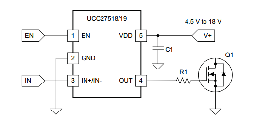
The UCC27518 and UCC27519 single-channel, high-speed, low-side gate driver device is capable of effectively driving MOSFET and IGBT power switches. Using a design that inherently minimizes shoot-through current, UCC27518 and UCC27519 are capable of sourcing and sinking high, peak-current pulses into capacitive loads offering rail-to-rail drive capability and extremely small propagation delay typically 17 ns.

The UCC27518 and UCC27519 provide 4-A source, 4-A sink (symmetrical drive) peak-drive current capability at VDD = 12 V. The UCC27518 and UCC27519 are designed to operate over a wide VDD range of 4.5 V to 18 V and wide temperature range of -40°C to 140°C. Internal Under Voltage Lockout (UVLO) circuitry on VDD pin holds output low outside VDD operating range.

Circuit Project: 4A High-Speed Low-side Gate Driver
Features
  • Low-Cost, Gate-Driver Device Offering Superior Replacement of NPN and PNP Discrete Solutions
  • Pin-to-Pin Compatible With TI’s TPS2828 and the TPS2829
  • 4-A Peak Source and 4-A Peak Sink Symmetrical Drive
  • Fast Propagation Delays (17-ns typical)
  • Fast Rise and Fall Times (8-ns and 7-ns typical)
  • 4.5-V to 18-V Single Supply Range
  • Outputs Held Low During VDD UVLO (ensures glitch free operation at power-up and power-down)
  • CMOS Input Logic Threshold (function of supply voltage with hysteresis)
  • Hysteretic Logic Thresholds for High Noise Immunity
  • EN Pin for Enable Function (allowed to be no connect)
  • Output Held Low when Input Pins are Floating
  • Input Pin Absolute Maximum Voltage Levels Not Restricted by VDD Pin Bias Supply Voltage
  • Operating Temperature Range of -40°C to 140°C
  • 5-Pin DBV Package (SOT-23)
Device Uses
  • Switch-Mode Power Supplies
  • DC-to-DC Converters
  • Companion Gate Driver Devices for Digital Power Controllers
  • Solar Power, Motor Control, UPS
  • Gate Driver for Emerging Wide Band-Gap Power Devices (such as GaN)
Read More..

Simple Low Drop 5V Regulator

A 4-cell pack is a convenient, popular battery size. Alkaline manganese batteries are sold in retail stores in packs of four, which usually provide sufficient energy to keep battery replacement frequency at a reasonable level. Generating 5 V from four batteries is, however, a bit tricky. A fresh set of four batteries has a terminal voltage of 6.4 V, but at the end of their life, this voltage is down to 3.2 V. Therefore, the voltage needs to be stepped up or down, depending on the state of the batteries. A flyback topology with a costly, custom designed transformer could be used, but the circuit in the diagram gets around the problem by using a flying capacitor together with a second inductor.

Circuit diagram:

The circuit also isolates the input from the output, allowing the output to go to 0 V during shutdown. The circuit can be divided conceptually into boost and buck sections. Inductor L1 and switch IC1 comprise the boost or step-up section, and inductor L2, diode D1 and capacitor C3 form the buck or step-down section. Capacitor C2 is charged to the input voltage, Vin, and acts as a level shift between the two sections. The switch toggles between ground and Vin+Vout , while the junction of L2, C2 and D1 toggles between –Vin and Vout +Vd1. Efficiency is directly related to the quality of the capacitors and inductors used.

Better quality capacitors are more expensive. Better quality inductors need not cost more, but normally take up more space. The Sanyo capacitors used in the prototype (C1–C3) specify a maximum ESR (effective series resistance) of 0.045 ½ and a maximum ripple current rating of 2.1 A. The inductors used specify a maximum DCR (direct current resistance) of 0.058 ½. Worst-case r.m.s. current through capacitor C2 occurs at minimum input voltage, that is, 400 mA at full load with an input voltage of 3 V. 
Read More..

Friday, September 12, 2014

Simple Low Power Switching Regulator Wiring diagram Schematic

This is the Simple Low Power Switching Regulator Circuit Diagram. A simple battery-powered switching regulator provides 5 V out from a 9-V source with 80% efficiency and 50 mA output capability. When Q1 is on, its collector voltage rises, forcing current through the inductor. The output voltage rises, causing A1`s output to rise. 

Low Power Switching Regulator Circuit Diagram


Simple

Q1 cuts off and the output decays through the load. The 100-pF capacitor ensures clean switching. The cycle repeats when the output drops1ow enough for A1 to turn on Ql. The 1-
Read More..

Tuesday, September 9, 2014

Low Cost Tone Control Circuit

Low

This cheap tone control schema provides a maximum cut and boost of around 10dB at 10K and 50Hz. Two potensiometer used to control the high frequency (treble) and low frequency (bass).

The first BC109C transistor (left hand side) is acting as a buffer. It provides the schema with a high input impedance, around 250k has a voltage gain of slightly less than unity. As the Baxendall tone control schema is a passive design, all audio frequencies are attenuated. The position of the controls and reactance of the capacitors alters the audio response. The last transistor provides a slight boost of about 3x. The output is designed to feed an amplifier with input impedance of 10k to 250k. Both tone controls should be linear type potentiometers.
Read More..

Sunday, August 24, 2014

Simple Low Drop 5V Regulator

A 4-cell pack is a convenient, popular battery size. Alkaline manganese batteries are sold in retail stores in packs of four, which usually provide sufficient energy to keep battery replacement frequency at a reasonable level. Generating 5 V from four batteries is, however, a bit tricky. A fresh set of four batteries has a terminal voltage of 6.4 V, but at the end of their life, this voltage is down to 3.2 V. Therefore, the voltage needs to be stepped up or down, depending on the state of the batteries. A flyback topology with a costly, custom designed transformer could be used, but the schema in the diagram gets around the problem by using a flying capacitor together with a second inductor.

Simple Low-Drop 5V Regulator  Circuit diagram:

Simple

The schema also isolates the input from the output, allowing the output to go to 0 V during shutdown. The schema can be divided conceptually into boost and buck sections. Inductor L1 and switch IC1 comprise the boost or step-up section, and inductor L2, diode D1 and capacitor C3 form the buck or step-down section. Capacitor C2 is charged to the input voltage, Vin, and acts as a level shift between the two sections. The switch toggles between ground and Vin+Vout , while the junction of L2, C2 and D1 toggles between –Vin and Vout +Vd1. Efficiency is directly related to the quality of the capacitors and inductors used.

Better quality capacitors are more expensive. Better quality inductors need not cost more, but normally take up more space. The Sanyo capacitors used in the prototype (C1–C3) specify a maximum ESR (effective series resistance) of 0.045 ½ and a maximum ripple current rating of 2.1 A. The inductors used specify a maximum DCR (direct current resistance) of 0.058 ½. Worst-case r.m.s. current through capacitor C2 occurs at minimum input voltage, that is, 400 mA at full load with an input voltage of 3 V. 
Read More..