Showing posts with label 4. Show all posts

Wednesday, October 29, 2014

TA8259H bassed 4 channel car amplifier Diagram Circuit


Using the TA8259H integrated circuit can be designed a very simple 4 ch BTL audio power amplifier for car audio application.
This IC can generate more high power: POUT MAX = 37 W as it is included the pure complementary PNP and NPN transistor output stage.

It is designed low distortion ratio for 4 ch BTL audio power amplifier, built-in Stand-by Function, Muting Function, Clip detector, and diagnosis circuit.
As you can see in the circuit diagram , this audio amplifier electronic project require extreme low external electronic parts .

Additionally, the AUX. amplifier is built-in, it can make the beep signal etc. output to 2 channels (OUT1 and 4).

Input voltage range that is accepted by this audio amplifier project is between 9 and 18 volt , but typically is required a 14,4 volts DC.
All speakers used with this amplifier circuit project , based on TA8259H IC must have a 4 ohms impedance .
Read More..

Monday, October 20, 2014

Build a 4 Transistor FM Transmitter Circuit Diagram

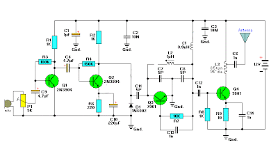
 4 Transistor FM Transmitter Circuit Diagram
 
 4 Transistor FM Transmitter Circuit Diagram

Build a  4 Transistor FM Transmitter Circuit Diagram. This 4 Transistor FM Transmitter Circuit Diagram provides an FM modulated signal with an output power of around 500mW. The input microphone pre-amp is built around a couple of 2N3904 transistors (Q1/Q2), and audio gain is limited by the 5k preset trim potentiometer. 

The oscillator is a colpitt stage, frequency of oscillation governed by the tank circuit made from two 5pF ceramic capacitors and the L2 inductor. The output stage operates as a Class D amplifier, no direct bias is applied but the RF signal developed across the 3.9uH inductor is sufficient to drive this stage. The emitter resistor and 1k base resistor prevent instability and thermal runaway in this stage.
Read More..

Wednesday, October 15, 2014

4 X 15 Watt Mini Power Amplifier

A lot of electronic circuits in the domain of audio amplifiers are already been published here. This circuit is a little different because it is a four channel amplifier. Each channel of this amplifier can deliver an output of 15Watts into a 4 ohm speaker. The amplifier can be operated from a single 12V DC supply and this makes it possible to use this amplifier in car audio applications too.

Circuit diagram :

4 X 15 Watt Mini Power Amplifier

The circuit is based on the 15W BTL X 2 channel audio power amplifier IC TA8215 from Toshiba. Even though chip is specifically designed for car audio applications it can be also used for home audio applications. Two TA8215 ICs are used here in order to obtain a 4 channel amplifier system. The circuit is designed almost exactly as per the application diagram in the ICs datasheet. Pins 7 and 19 are the Vcc pins of the ICs internal integrated power amplifier stages and these pins are connected to the positive supply. Pin 9 is the Vcc pin for ICs internal preamplifier and it is also connected to the positive supply. Pins 13 and 14 are the internal power amplifiers ground pins and they are tied together and connected to the ground. 

The internal preamplifier’s ground pin (pin5) is connected to the common ground through a 10 Ohm resistor which makes the input ground separated from the common ground by a resistance of 10 ohms and this improves the noise rejection. The 100uF capacitor works as a power supply de-coupler. The resistor networks connected to the output lines of each amplifier improves the high frequency stability. The variable resistors (R3, R4, R12 and R13) works as the volume controller for the corresponding channels.

Notes :
  • Assembling the circuit on a good quality PCB is a must for obtaining optimum sound quality.
  • Use 12V DC for powering the circuit.
  • The ICs must be fitted with adequately sized heat sinks.
  • R3, R4, R12 and R13 serves as volume controllers.
  • K1 to K4 can be 4 Ohm, 20W speakers.
  • This amplifier circuit can be used in a variety of applications such as car audio systems, home theater systems, personal audio systems, public address systems etc.
Read More..

Thursday, September 18, 2014

4 x 45 W power amplifier

General description

The TDA8593J is a complementary quad BTL audio power amplifier made in BCDMOS technology. It contains four independent amplifiers in Bridge Tied Load (BTL) configuration. Through the I2C-bus, the diagnostic information of each amplifier and speaker can be read separately. Both front and both rear channel amplifiers can be configured independently in line driver mode with a gain of 20 dB.

Features

  • I2C-bus control
  • Hardware programmable I2C-bus address
  • Can drive a 2 Ω load with a battery voltage of up to 16 V and a 4 Ω load with a battery voltage of up to 18 V
  • DC-load detection: open, short and present
  • AC-load (tweeter) detection
  • Programmable clip detection: 1 % or 3 %
  • Programmable thermal protection pre-warning
  • Independent short-circuit protection per channel
  • Low gain line driver mode (20 dB)
  • Loss-of-ground and open VP safe
  • All outputs protected from short-circuit to ground, to VP, or across the load
  • All pins protected from short-circuit to ground
  • Soft thermal clipping to prevent audio holes
  • Low battery detection.


Circuit Diagram
Circuit diagram for TDA8593

PCB layout of test and application circuit; components bottom

 PCB layout of test and application circuit; copper layer bottom

PCB layout of test and application circuit; components top

 PCB layout of test and application circuit; copper layer top


Read More..

Saturday, September 13, 2014

Part 4 Contact info and web adresses of integrated circuits power audio amplifiers manufacturers


Mag- Magnatec (Semelab Subdivision)
Semelab Plc. Coventry Road, Lutterworth, UK. Phone: +44-1455-552505
http://www..semelab.co.uk

Max- Maxim Integrated Products
120 San Gabrial Sunnyvale, CA 94086, USA. Phone: +1-800-998-8800
http://www.maxim-ic.com

Mcp- Microchip Technology Inc.
2355 West Chandler Blvd. Chandler, AZ 85224-6199, USA. Phone: 480-792-7200
http://www.microchip.com

Mit- Mitsubishi Electric Co. Ltd. (ICs manufacture is handed to Renssas Ltd.)
2-3 Marunouchi, 2-chome J 100 Chiyoda-Ku, Tokyo, Japan. Phone: +81-3-3218-2863
http://www.mitsubishichips.com

Mot- Motorola Inc. (ICs manufacture is handed to ON Semiconductor)
6501 William Cannon Drive W Austin, TX 78735 USA. Phone: +1-512-891-2000
http://www.motorola.com

Mps- Monolithic Power Systems
6409 Guadalupe Mines Road, San Jose, CA 95120, USA. Phone: 408-826-0600
http://www.monolithicpower.com

Mts- Mitsumi Electric Co. Ltd.
8-8-2, Kokuryo-cho, Chofu-chi, Tokyo 182-8557, Japan. Phone: (03)3489-5333
http://www.mitsumi.co.jp

Msk- M.S.Kennedy Corp.
4707 Dey Road Liverpool, N.Y. 13088 USA . Phone (315) 701-6751
www.mskennedy.com

Mul- Mullard LTD (Is not a current ICs manufacturer)
New Road Mitcham, Surrey England CR4 4XY. Telex: 264341
NEC Electronics Inc. (Nippon Electrical Company)
NEC Building 7-1, Shiba 5-chome, Minato-ku Tokyo, Japan. Phone: +81-3-3454-1111
http://www.ic.nec.co.jp

NJR- New Japan Radio Co., Ltd.
Arvco Tower 17F, 1-8-1, Shimomeguro, Meguro-ku, Tokyo 153, Japan.
Phone: +81-3-5434-8335
http://www.njr.com

Npc- Nippon Precision Circuits Inc.
4-3, Fukuzumi 2-chome, Koto-ku, Tokyo 135-8430, Japan. Phone:+81-3-3642-6661
http://www.npc.co.jp/453

NSC- National Semiconductor Corp.
North America PO Box 7643 Mount Prospect, IL 60056-7643, USA.
Phone: +1-800-628-7364, ext 305
http://www.national.com

NTE Electronics Inc.
44 Farrand Street, Bloomfield, NJ 07003, USA. Phone: 800-631-1250
http://www.nteinc.com

Nxp- NXP Semiconductors
PO Box 80073, 5600 KA Eindhoven, Netherlands. Phone: +31 40 27 45678
http://www.nxp.com

Oki Semiconductor Inc.
785 N Mary Avenue Sunnyvale, CA 94086, USA .Phone: +1-408-720-1900
http://www.okisemi.com

Omn- Omnirel (Acquired by International Rectifier)
 205 Crawford Street, Leominster, MA 01453 USA. Phone: (508) 534-5776
http://www.omnirel.com

Ons- ON Semiconductor (Motorola semiconductors subdivision)
Japan Customer Focus Center 4321 NishiGotanda, Shinagawaku, Tokyo, Japan
Phone: 81357402745
http://onsemi.com

Pan- Panasonic Electronics Corp.
1 Kotari-Yakemashi, Nagaokakyo, Kyoto 617, Japan. Phone: 075/921-8151
http://www.mec.panasonic.co.jp

Pch- PointChips Co. Ltd.
4FL., Dabong Tower Bldg. 890-12, Daechi-Dong, Kangnam-Gu, Seoul 135-280, Korea
Phone: 82-2-508-2443
http://www.pointchips.com

Phi- Philips GmbH (ICs manufacture is handed to NXP Semconductor)
Hammerbrookstrasszlige 69 D-20097 Hamburg, Germany. Phone: +49-40-23536-0
http://www.philips.com

Pjn- Promax-Johnton
(There is no accesible padding information)
http://www.p-johnton.com

Pls- GEC Plessey Semiconductor
(Is not a current ICs manufacturer)
Pnr- Pioneer Not the manufacturer of ICs
Will use custom IC with Pioneer type marking
Ptc- Princeton Technology Corp.
2F, No. 233-1, Baociao Road, Sindian City, Taipei 23145, Taiwan, R.O.C.
Phone: 886-2-66296288
http://www.princeton.com.tw

Rca- RCA Corporation (Is not a current ICs manufacturer)
Route 202, Sommerville, NJ 08876, USA. Phone: 201/685-6423
http://www.rca.com
Ren- Renessas Ltd.
Nippon Bldg., 2-6-2, Ohte-machi, Chiyoda-ku, Tokyo 100-0004, Japan,
Phone: 852-2424-9127
http://www.renesas.com


Read More..

Wednesday, September 10, 2014

4 5V To 12V DC


This ic 4.5V to 12V boost schema.You all can get lots of advantages through this schema.Here I have used famous IC LM2698.


Note

# input supply voltage range is 2.2V to 17V DC and outputs ranging from 2.2V to 17V DC

# IC can deliver only up to 400mA.So dont connect lodes more than that

# Build this schema on a PCB
Read More..

Saturday, September 6, 2014

How to Build a 2 to 4 Wire Audio Converter

This audio converter schema maintains 40 dB of isolation between the two halves of entry and exit of a four-line son, while allowing a line connecting two son. A balancing potentiometer, R, adjusts the gain of zero lC2to crossing the inlet to the outlet .

The adjustment is done in terms of work just after installation by inserting a 1 kHz tone at the entrance of four son and setting R to the minimum output signal 82-ohm dummy-load resistor is placed between two wire terminals .

 2 to 4 Wire Audio Converter Circuit Diagram

How

Read More..

Monday, August 25, 2014

4 x 30W QUAD BRIDGE CAR RADIO AMPLIFIER

Description

The TDA7383 is a new technology class AB Audio Power Amplifier in Flexiwatt 25 package designed for high end car radio applications.

Circuit Diagram
4 x 30W QUAD BRIDGE CAR RADIO AMPLIFIER


Read More..

Tuesday, August 19, 2014

4 Bit Analogue to Digital Converter Wiring diagram Schematic

The operation of the converter is based on the weighted adding and transferring of the analogue input levels and the digital output levels. It consists of comparators and resistors. In theory, the number of bits is unlimited, but each bit needs a comparator and several coupling resistors. The diagram shows a 4-bit version. The value of the resistors must meet the following criteria:
  • R1:R2 = 1:2;
  • R3:R4:R5 = 1:2:4;
  • R6:R7:R8:R9 = 1:2:4:8.
The linearity of the converter depends on the degree of precision of the value of the resistors with respect to the resolution of the converter, and on the accuracy of the threshold voltage of the comparators. This threshold level must be equal, or nearly so, to half the supply voltage. Moreover, the comparators must have as low an output resistance as possible and as high an input resistance with respect to the load resistors as feasible. Any deviation from these requirements affects the linearity of the converter adversely.

4-Bit Analogue to Digital Converter Circuit Diagram

4-Bit
4-Bit Analogue to Digital Converter Circuit Diagram

If the value of the resistors is not too low, the use of inverters with an FET (field-effect transistor) input leads to a near-ideal situation. In the present converter, complementary metal-oxide semiconductor (CMOS) inverters are used, which, in spite of their low gain, give a reasonably good performance. If standard comparators are used, take into account the output voltage range and make sure that the potential at their non-inverting inputs is set to half the supply voltage. If high accuracy is a must, comparators Type TLC3074 or similar should be used. This type has a totem-pole output. The non-inverting inputs should be interlinked and connected to the tap of a a divider consisting of two 10 kΩ resistors across the supply lines. It is essential that the converter is driven by a low-resistance source. If necessary, this can be arranged via a suitable op amp input buffer. The converter draws a current not exceeding 5 mA.
Read More..

Monday, August 11, 2014

Amplifier Circuit based 4 Transistors

Amplifier Circuit based 4 Transistors diagram


Above diagram very simple and easy to build class AB audio amplifier schema which is working with 4 transistors. In class AB operation each output device performs more than half of the input signal cycle. Up to 78% effectiveness is possible with class AB designs and cross over distortion is minimized. The schema shown here is appropriate for small radio receivers, audio players, intercom, phone etc.

Transistor Q1 with its connected parts is wired as a pre-amplifier stage. The audio input is coupled to the base of Q1 through resistor R1 and capacitor C1. Resistor R3 delivers collector to base bias for Q1 and C3 is an AC by pass capacitor for the collector resistor R4. Collector to base biasing is a great method of biasing for diagram like this because it provides enough negative feedback, prevents thermal runway and stabilizes the operating point. The second stage will be the driver stage for the push pull pair. Q2 with its connected parts carry out this job. This stage can also be collector to base biased, and its input is coupled towards the output from the pre-amplifier stage using capacitor C2. Resistor R8 limits the collector present of Q2.The third stage is the class AB push pull section comprising of transistors Q3 and Q4. Diodes D1 and D2 provides the bias voltage for the push pull stage. The output from the amplifier is coupled to the loud speaker through the capacitor C4. C5 and C6 are power supply filter capacitors.

Notes:
  1. The schema can be assembled on a vero board.
  2. K1 may be an 8 ohm/5Wof loud speaker.
  3. C6 must be grounded near towards the Q1 and C5 should be grounded near to the loud speaker ground. This reduces noise.
  4. Use 5V DC power supply for powering the schema.
Read More..