Showing posts with label 1. Show all posts
Showing posts with label 1. Show all posts
Tuesday, November 18, 2014
Power Supply Variable 1 3V 12 2V 1A Circuit
Power supply circuit to generate output below were variations between 1.3V DC to 12.2V DC with 1A current. In addition, the power supply circuit is also equipped with over-current protection or shield against belebih flow. Power supply circuit is very simple, but the quality is quite good, made her basiskan regulator IC LM723 is a pretty legendary.

Description:
R2 to set the output voltage. The maximum current is determined by R3, over-current protection circuit inside the LM723 to detect the voltage on R3, if it reaches 0.65 V, the voltage output will be off her. So the current through R3 can not exceed 0.65 / R3 although output short-circuit in his.
C3 and C4 are ceramic capacitors, as much as possible directly soldered to the PCB, this is because the LM723 is prone to oscillation that is not cool.
LM723 works with 9.5V input voltage to 40 V DC and the LM723 can generate its own current of 150mA when the output voltage is not more than 6-7V under input voltage.
Specifications:
Output (value estimated):
Vmin = (R4 + R5) / (R5 * 1.3)
Vmax = (7.15 / R5) * (R4 + R5)
Imax = 0.65/R3
Max. Power on R3: 0.42/R3
Min. DC Input Voltage (pin 12 to pin 7): Vmax + 5
Component List:
B1 40V/2.5A
C1 2200uF (3300uF even better)
C2 4.7uF
C3 100nF
C4 1NF
C5 330nF
C6 100uF
Green LED D1
D2 1N4003
F1 0.2A F
F2 2A M
IC1 LM723 (in a DIL14 plastic package)
R1 1k
R2 Pot. 5k
R3 0.56R/2W
R4 3.3k
R5 4.7k
S1 250V/1A
T1 2N3055 on a heatsink 5K / W
TR1 220V/17V/1.5

Sunday, November 2, 2014
ADJUSTABLE 1 5A STEP DOWN 1 5MHz SWITCHING REGULATOR ELECTRONIC DIAGRAM

ADJUSTABLE 1.5A STEP DOWN 1.5MHz SWITCHING REGULATOR ELECTRONIC DIAGRAM
However, an Adjustable 1.5A Step Down 1.5 MHz switching regulator circuit can also be used to overcome such problem. It uses ST1S03 step down DC-DC converter. The ST1S03 can also be used to power low-voltage digital core in HDD application .
With input voltage range 3V to 16V, the ST1S03 can gives current up to 1.5A. The circuit can use tiny surface-mount components due to an high switching frequency (1.5 MHz). Resistor divider is used to set the output voltage value. Components needed to build the divided are capacitors (2 pieces), schottky diode (1 piece), and inductor (1 piece).
Thursday, October 23, 2014
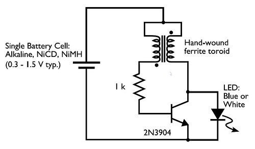
0 3 to 1 5V LED Flashlight

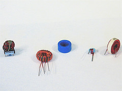
Its a little wisp of a circuit that allows you to drive a blue or white LED from a low voltage. Normally, if you want to light up a blue or white LED you need to provide it with 3 - 3.5 V, like from a 3 V lithium coin cell. But a 1.5 V battery like a AA cell simply will not work. But using the Joule Thief, it works like a charm. Not only does it work with a brand new battery, but it works until the battery is nearly dead-- down to 0.3 V. Thats well below the point where your other toys will tell you the battery is dead, so it can steal every last joule of energy from the battery (hence the name). To learn how to make one, watch the video, which is available in a variety of formats.


Friday, September 19, 2014
Generation of 1 Sec Pulses Spaced 5 Sec Apart
This circuit using a dual-timer NE556 can produce 1Hz pulses spaced 5 seconds apart, either manually or automatically. IC NE556 comprises two independent NE555 timers in a single package. It is used to produce two separate pulses of different pulse widths, where one pulse initiates the activation of the second pulse. The first half of the NE556 is wired for 5-second pulse output. When slide switch S2 is in position ‘a’, the first timer is set for manual operation, i.e. by pressing switch S1 momentarily you can generate a single pulse of 5-second duration. When switch S2 is kept in ‘b’ position, i.e. pins 6 and 2 are shorted, timer 1 in NE556 triggers by itself.
The output of the first timer is connected to trigger pin 8 of second timer, which, in turn, is connected to a potential divider comprising resistors R4 and R5. Resistor R1, preset VR1, resistor R2, preset VR2, and capacitors C2 and C5 are the components determining time period. Presets VR1 and VR2 permit trimming of the 5-second and 1-second pulse width of respective sections. When switch S2 is in position ‘a’ and switch S1 is pressed momentarily, the output at pin 5 goes high for about 5 seconds. The trailing (falling) edge of this 5-second pulse is used to trigger the second timer via 0.1µF capacitor C6.
Circuit diagram: This action results in momentarily pulling down of pin 8 towards the ground potential, i.e. ‘low’. (Otherwise pin 8 is at 1/2 Vcc and triggers at/below 1/3 Vcc level.) When the second timer is triggered at the trailing edge of 5-second pulse, it generates a 1-second wide pulse. When switch S2 is on position ‘b’, switch S1 is disconnected, while pin 6 is connected to pin 2. When capacitor C is charged, it is discharged through pin 2 until it reaches 1/3Vcc potential, at which it is retriggered since trigger pin 6 is also connected here. Thus timer 1 is retriggered after every 5-second period (corresponding to 0.2Hz frequency). The second timer is triggered as before to produce a 1-second pulse in synchronism with the trailing edge of 5-second pulse.
This circuit is important wherever a pulse is needed at regular intervals; for instance, in ‘Versatile Digital Frequency Counter Cum Clock’ construction project published in EFY Oct. ’97, one may use this circuit in place of CD4060-based circuit. For the digital clock function, however, pin 8 and 12 are to be shorted after removal of 0.1µF capacitor and 10-kilo-ohm resistors R4 and R5.
Read More..
The output of the first timer is connected to trigger pin 8 of second timer, which, in turn, is connected to a potential divider comprising resistors R4 and R5. Resistor R1, preset VR1, resistor R2, preset VR2, and capacitors C2 and C5 are the components determining time period. Presets VR1 and VR2 permit trimming of the 5-second and 1-second pulse width of respective sections. When switch S2 is in position ‘a’ and switch S1 is pressed momentarily, the output at pin 5 goes high for about 5 seconds. The trailing (falling) edge of this 5-second pulse is used to trigger the second timer via 0.1µF capacitor C6.
Circuit diagram:
 This action results in momentarily pulling down of pin 8 towards the ground potential, i.e. ‘low’. (Otherwise pin 8 is at 1/2 Vcc and triggers at/below 1/3 Vcc level.) When the second timer is triggered at the trailing edge of 5-second pulse, it generates a 1-second wide pulse. When switch S2 is on position ‘b’, switch S1 is disconnected, while pin 6 is connected to pin 2. When capacitor C is charged, it is discharged through pin 2 until it reaches 1/3Vcc potential, at which it is retriggered since trigger pin 6 is also connected here. Thus timer 1 is retriggered after every 5-second period (corresponding to 0.2Hz frequency). The second timer is triggered as before to produce a 1-second pulse in synchronism with the trailing edge of 5-second pulse.
 This circuit is important wherever a pulse is needed at regular intervals; for instance, in ‘Versatile Digital Frequency Counter Cum Clock’ construction project published in EFY Oct. ’97, one may use this circuit in place of CD4060-based circuit. For the digital clock function, however, pin 8 and 12 are to be shorted after removal of 0.1µF capacitor and 10-kilo-ohm resistors R4 and R5.
Thursday, September 4, 2014
LM 386 Amplifier circuit 1 W
LM 386 general description:
This circuit is a signal line so that you reinforce a small speaker can drive with. The LM 386 is a number of versions available. The LM 386N-1 can deliver a power of 325 mW, the LM 386N-2500 mW, the LM 386N-3700 mW and LM 386N-4 can deliver one watt output. All versions can be used in the circuit. Using S1 is a bass boost (extra bass enhancement) to turn. The state is drawn from the bass-boost.
LM 386 circuit diagram:

LM 386 partlist:
R1 = 10 kR 2 = 10 Ω
P1 = 10 k
C1 = 100 nF
C2 = 47 nF
C3 = 470 uF
C4 = 10 uF
C5 = 33 nF
IC1 = LM 386
S1 = switch
Wednesday, September 3, 2014
TDA2822 made for 5 1 audio amplifier system
Skema Rangkaian Circuit combination of the 3 IC TDA2822 above can be used for 5.1 audio power amplifier system with low power output . The input signal used is analog signal not digital (SPDIF) , so it needed some input to the jack input. The speakers are suitable for use have impedance 8 Ohms , and with power 4 Watt, to Left , Right , Rear pair , center , and subwoofer speakers. To run this circuit , is also required circuit for volume control as tone control.

Component and technical Information :
C1-C6 : 220uF/25V
C7-C9 : 47uF/16 V
IC : TDA2822 x3
CON-1: VCC +12volts DC
CON-2: Ground
CON-3: Left Speaker
CON-4: Right Speaker
CON-5: Rear Speaker
CON-6: Rear Speaker
CON-7: Center Speaker
CON-8: Subwoofer Speaker
X1-1:Ground
X1-2:Subwoofer Input
X1-3:Center Input
X1-4:Rear Input
X1-5:Rear Input
X1-6:Right Input
X1-7:Left Input
See this Printed circuit board below:

circuit and PCB Design use Cadsoft Eagle Software
Subscribe to:
Posts (Atom)
