Showing posts with label how. Show all posts
Showing posts with label how. Show all posts
Friday, November 14, 2014
How to Build a UPS for USB devices
Portable systems often include circuitry that derives power from an external source, such as USB. When the system disconnects from the USB supply, a battery takes over and supplies current via a dc/dc converter. A diode-OR connection (Figure 1 offers the easiest way to ensure that the supply voltage doesnt sag during this switchover to the battery. The diodes forward voltage drop, however, can reduce battery life and efficiency.


The single-cell, boost-converter circuit with external PFET (Figure 2) is an improvement over the diode-OR connection. The PFET, Q1, coupled with IC1s internal gain block, forms a linear regulator. The USB power supply has a diode-OR connection to Q1s source. Setting the boost converters output to 3.4V allows the drain of Q1 to regulate to 3.3V. This configuration produces negligible loss in Q1. The bus-supply voltage available to USB devices ranges from 4.4 to 5.25V.
When you connect the bus, it forward-biases D1 and causes the boost converter to idle. The converter continues to idle as long as its output remains above the 3.4V regulation point. The bus supply serves the load and activates the current source to charge the battery.

Adjusting R1 allows you to set the current-source output to charge the nickel-metal-hydride cells at a level one-tenth the batterys capacity. Disconnecting the circuit from the USB supply causes the boost converter to cease idling and supply current to the load via the battery. Figure 3 shows that the load current suffers no interruption during a switchover from USB to battery.
Read More..
A diode-OR connection is effective but lossy.
A boost-converter circuit is an improvement over the simple diode-OR connection.
The single-cell, boost-converter circuit with external PFET (Figure 2) is an improvement over the diode-OR connection. The PFET, Q1, coupled with IC1s internal gain block, forms a linear regulator. The USB power supply has a diode-OR connection to Q1s source. Setting the boost converters output to 3.4V allows the drain of Q1 to regulate to 3.3V. This configuration produces negligible loss in Q1. The bus-supply voltage available to USB devices ranges from 4.4 to 5.25V.
When you connect the bus, it forward-biases D1 and causes the boost converter to idle. The converter continues to idle as long as its output remains above the 3.4V regulation point. The bus supply serves the load and activates the current source to charge the battery.
Adjusting R1 allows you to set the current-source output to charge the nickel-metal-hydride cells at a level one-tenth the batterys capacity. Disconnecting the circuit from the USB supply causes the boost converter to cease idling and supply current to the load via the battery. Figure 3 shows that the load current suffers no interruption during a switchover from USB to battery.

Monday, October 27, 2014
How Regulator with 2 Photocoupler
Working of Regulator with 2 Photocoupler that is :
- Photocoupler N901 - used as a coupling-off control on the regulator by mikrokontrol. Which is set high and low voltage B + (st-by at the B + voltage is low). Control of the pin-37 POWER mikrokontrol → V610 → VD913 V908 → N901.
- Photocoupler N903 - used to control on-off the regulator of X-ray circuit protector. X-ray protector circuit of flyback → VD451 → VD452 → SCR VS472. If the flyback voltage regulator over the job will automatically be turned off by N903
- To disable the X-ray circuit protector, it can be temporarily removed photocoupler N903 first. In normal conditions the voltage at the transistor V474 should be zero.

 |
| Regulator Schematics |
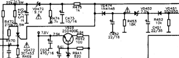
- Disable by removing the first circuit protectors N903
- Check the voltage of 300V
- Check all transistors
- Check the start voltage of 300V by R909 >> R906 to the base of transistor power regulator
- Check the feedback C910 >> R904 (to oscillate)
Thursday, October 16, 2014
How to Lights Control for Model Cars
The author gave his partner a radio controlled (RC) model car as a gif t. She found it a lot of fun, but thought that adding realistic lights would be a definite improvement. So the author went back to his shed, plugged in his soldering iron, and set to work equipping the car with realistic indicators, headlights, tail lights and brake lights.
Lights Control for Model Cars Circuit Diagram

The basic idea was to tap into the signal from the radio control receiver and, with a bit of help from a microcontroller, simulate indicators using flashing yellow LEDs and brake lights using red LEDs. Further red LEDs are used for the tail lights, and white LEDs for the headlights. Connectors JP4 and JP5 (channel 0) are wired in parallel, as are JP6 and JP7 (channel 1), allowing the circuit to be inserted into the servo control cables for the steering and drive motor respectively. The ATtiny45 micro-controller takes power from the radio receiver via diode D1. T1 and T2 buffer the servo signals to protect IC1’s inputs from damage.
IC1 analyses the PWM servo signals and gen-erates suitable outputs to switch the LEDs via the driver transistors. T3 drives the two left indicators (yellow), T4 the two right indica-tors, and T5 the brake LEDs (red). The red tail lights (JP2-8 and JP2-8) and the white head-lights (JP2-9 and JP2-10) are lit continuously. The brake lights are driven with a full 20 mA, so that they are noticeably brighter than the tail lights, which only receive 5 mA. If you wish to combine the functions of tail light and brake light, saving t wo red LEDs, sim-ply connect pin 10 of JP2 to pin 14 and pin 12 to pin 16. Then connect the two combined brake/tail LEDs either at JP2-5 and JP2-6 or at JP2-7 and JP2-8.
JP3 is provided to allow the use of a separate lighting supply. This can either be connected to an additional four-cell battery pack or to the main supply for the drive motor. The val-ues given for resistors R8 to R17 are suitable for use with a 4.8 V supply. JP2 can take the form of a 2x10 header.
As usual the sof t ware is available as a free download from the Elektor web pages accom-panying this article[1], and ready-programmed microcontrollers are also available. The microcontroller must be taught what servo signals correspond to left and right turns, and to full throttle and full braking. First connect the fin-ished circuit to the radio control electronics in the car, making sure everything is switched of f. Fit jumper JP1 to enable configuration mode, switch on the radio control transmit-ter, set all proportional controls to their cen-tre positions, and then switch on the receiver. The indicator LEDs should first flash on both sides. Then the car will indicate left for 3 s: during this time quickly turn the steering on the radio control transmitter fully to the left and the throt tle to full reverse (maximum braking).
Hold the controls in this position until the car starts to indicate right. Then set the controls to their opposite extremes and hold them there until both sides flash again. Now, if the car has an internal combustion engine (and so cannot go in reverse), keep the throttle control on full; if the car has an electric motor, set the throttle to full reverse. Hold this position while both sides are flashing.
JP3 is provided to allow the use of a separate lighting supply. This can either be connected to an additional four-cell battery pack or to the main supply for the drive motor. The val-ues given for resistors R8 to R17 are suitable for use with a 4.8 V supply. JP2 can take the form of a 2x10 header.
As usual the sof t ware is available as a free download from the Elektor web pages accom-panying this article[1], and ready-programmed microcontrollers are also available. The microcontroller must be taught what servo signals correspond to left and right turns, and to full throttle and full braking. First connect the fin-ished circuit to the radio control electronics in the car, making sure everything is switched of f. Fit jumper JP1 to enable configuration mode, switch on the radio control transmit-ter, set all proportional controls to their cen-tre positions, and then switch on the receiver. The indicator LEDs should first flash on both sides. Then the car will indicate left for 3 s: during this time quickly turn the steering on the radio control transmitter fully to the left and the throt tle to full reverse (maximum braking).
Hold the controls in this position until the car starts to indicate right. Then set the controls to their opposite extremes and hold them there until both sides flash again. Now, if the car has an internal combustion engine (and so cannot go in reverse), keep the throttle control on full; if the car has an electric motor, set the throttle to full reverse. Hold this position while both sides are flashing.
Friday, September 26, 2014
How to Design and Make Transformer at Home
Almost every electronic circuit needs a separate power supply, which may be a battery or a rectified power supply. Here we will deal with the design and making of small transformers that are normally used in conjunction with mains-operated power supplies.
This will help electronic hobbyists to design and construct their own transformers according to their needs. In the following pages, a simplified design procedure is given so as to obtain satisfactorily designed transformers. However, the design procedure is often a matter of trial and error.
The tables provided here cut calculations short and help the designer to choose the proper size of wire or core lamination. Only relevant data and calculations are provided so that the designer is not confused by unnecessary details.
The transformer
A transformer has two or more windings of insulated copper wire over an iron core. They are: one primary winding and one or more secondary windings. Each winding is electrically isolated from the other, but they are magnetically coupled with the help of a laminated iron core. Small transforrners have a shell type construction, i.e. the windings are surrounded by the core as shown in Fig. 1. The power delivered by the secondary is actually transferred from the primary, but at a voltage level determined by the turns ratio of the two windings.
Making the Preliminary Transformer design
As the first step to the design of a transformer, the primary and secondary voltage ratings and the secondary current rating must be clearly stated. Then decide on the core material to be used: ordinary steel stampings or cold rolled grain oriented (CRGO) stampings. CRGO has a higher allowable flux density and lower losses.
Core area = 1.l52 x root of (Output voltage x output current) sq. cm.
For transformers with multiple secondaries, the sum of the output volt-amp. product of each winding is to be used. The number of tums on the primary and secondary windings is decided by the turns per volt ratio as:
Turns per volt = 1/ (4.44 X l0^-4 frequency x core area x flux density)
Here, the frequency is 50Hz for Indian domestic mains supply. The flux density can be taken as about 1.0 Weber/ sq. m. for ordinary steel stampings and about 1.3 Weber/ sq. m. for CRGO stampings.
Primary winding design
The current in the primary winding is given by:
Primary Current = Sum of (output volts x output amps)/(Primary volts x efficiency)
The efficiency of small transformers varies between 0.8 to 0.96. A value of 0.87 can be used for ordinary transformers. The proper wire size has to be selected for the winding. The wire diameter depends on the current to be supplied by the winding and the allowable current density of the wire. The current density may be as high as 233 amps/ sq. cm. in small transformers and as low as 155 amps/sq. cm. in large ones. Usually, a value of 200 amps/ sq. cm. can be taken, on whose basis Table 1 is given.
The number of tums in the primary winding is given by:
Primary turns = Turns per volt x primary volts.
The space taken up by the winding will depend on the insulation thickness, method of winding and the wire diameter. Table I gives the approximate values of the turns per square cm. from which we can estimate the window area occupied by the primary winding.
Primary Winding Area = Primary turns/Turns per sq. cm. from Table1
Secondary winding design
Since we have assumed that we know the secondary current rating, we can find out the wire size for the secondary winding by referring to Table 1 directly.
The number of turns on the secondary is calculated in the same way as for the primary, but about 3% extra turns are to be added to compensate for the internal drop of secondary voltage of the transformer, upon loading. Thus,
Secondary Turns = 1.03 (turns per volt x secondary volts)
The window area required for secondary winding is found from Table1 as
Secondary window area = Secondary Turns/Turns per sq. cm from Table1

Core size
The main criterion in selecting the core is the total window area of winding space available.
Total window area = Primary window area + sum of secondary window areas + space for former and insulation
Some extra area is required to accommodate the former and insulation between windings. The actual amount of extra area varies, although 30% may be taken to start with but may have to be modified later. The suitable core sizes having a larger window area are selected from Table ll. . Taking into account the gap between laminations while stacking them (the core stacking factor taken as 0.9), we have
Gross core area = Core Area/0.9 sq.cm.
ln general, a square central limb is preferred. For this, the width of the tongue of lamination is
Tongue width = root of Gross core area cm.
Now refer to Table ll again and finally select the proper i core size, with sufficient window area and a close value of the tongue width as calculated. Adjust the stack height as required to obtain the required core section.
Stack height = Gros core area/Actual tongue width cm.
The stack should not be much less than the tongue width but may be more. However, it should not be more than 1% times the tongue width.

How to Design and Make a Transformer finally
The windings are wound on an insulating former which .fits over the center limb of the core.The primary is usually wound first, then the secondary, with insulation between windings, A final insulating layer is provided over the windings to protect them from mechanical damage. When thin wires are used, their ends must be soldered to thicker wires for bringing the terminals outside the former. The laminations are assembled over the former with alternate laminations reversed in assembly. The laminations must be held together tightly by a suitable clamping frame or by screws (if holes are provided in the laminations).

Shield
lt is a good practice to use an electrostatic shield between the primary and secondary windings to prevent disturbances from passing through to the secondary from the primary. The shield is made out of a copper foil which is wound between the two windings for slightly over a tum. Insulation must be provided along the length of the foil and care taken so that the- two ends of the foil do not touch each other. A wire soldered to the foil is bought out and connected to the ground.

A practical design example can be witnessed below:

This will help electronic hobbyists to design and construct their own transformers according to their needs. In the following pages, a simplified design procedure is given so as to obtain satisfactorily designed transformers. However, the design procedure is often a matter of trial and error.
The tables provided here cut calculations short and help the designer to choose the proper size of wire or core lamination. Only relevant data and calculations are provided so that the designer is not confused by unnecessary details.
The transformer
A transformer has two or more windings of insulated copper wire over an iron core. They are: one primary winding and one or more secondary windings. Each winding is electrically isolated from the other, but they are magnetically coupled with the help of a laminated iron core. Small transforrners have a shell type construction, i.e. the windings are surrounded by the core as shown in Fig. 1. The power delivered by the secondary is actually transferred from the primary, but at a voltage level determined by the turns ratio of the two windings.
Making the Preliminary Transformer design
As the first step to the design of a transformer, the primary and secondary voltage ratings and the secondary current rating must be clearly stated. Then decide on the core material to be used: ordinary steel stampings or cold rolled grain oriented (CRGO) stampings. CRGO has a higher allowable flux density and lower losses.
Core area = 1.l52 x root of (Output voltage x output current) sq. cm.
For transformers with multiple secondaries, the sum of the output volt-amp. product of each winding is to be used. The number of tums on the primary and secondary windings is decided by the turns per volt ratio as:
Turns per volt = 1/ (4.44 X l0^-4 frequency x core area x flux density)
Here, the frequency is 50Hz for Indian domestic mains supply. The flux density can be taken as about 1.0 Weber/ sq. m. for ordinary steel stampings and about 1.3 Weber/ sq. m. for CRGO stampings.
Primary winding design
The current in the primary winding is given by:
Primary Current = Sum of (output volts x output amps)/(Primary volts x efficiency)
The efficiency of small transformers varies between 0.8 to 0.96. A value of 0.87 can be used for ordinary transformers. The proper wire size has to be selected for the winding. The wire diameter depends on the current to be supplied by the winding and the allowable current density of the wire. The current density may be as high as 233 amps/ sq. cm. in small transformers and as low as 155 amps/sq. cm. in large ones. Usually, a value of 200 amps/ sq. cm. can be taken, on whose basis Table 1 is given.
The number of tums in the primary winding is given by:
Primary turns = Turns per volt x primary volts.
The space taken up by the winding will depend on the insulation thickness, method of winding and the wire diameter. Table I gives the approximate values of the turns per square cm. from which we can estimate the window area occupied by the primary winding.
Primary Winding Area = Primary turns/Turns per sq. cm. from Table1
Secondary winding design
Since we have assumed that we know the secondary current rating, we can find out the wire size for the secondary winding by referring to Table 1 directly.
The number of turns on the secondary is calculated in the same way as for the primary, but about 3% extra turns are to be added to compensate for the internal drop of secondary voltage of the transformer, upon loading. Thus,
Secondary Turns = 1.03 (turns per volt x secondary volts)
The window area required for secondary winding is found from Table1 as
Secondary window area = Secondary Turns/Turns per sq. cm from Table1
Core size
The main criterion in selecting the core is the total window area of winding space available.
Total window area = Primary window area + sum of secondary window areas + space for former and insulation
Some extra area is required to accommodate the former and insulation between windings. The actual amount of extra area varies, although 30% may be taken to start with but may have to be modified later. The suitable core sizes having a larger window area are selected from Table ll. . Taking into account the gap between laminations while stacking them (the core stacking factor taken as 0.9), we have
Gross core area = Core Area/0.9 sq.cm.
ln general, a square central limb is preferred. For this, the width of the tongue of lamination is
Tongue width = root of Gross core area cm.
Now refer to Table ll again and finally select the proper i core size, with sufficient window area and a close value of the tongue width as calculated. Adjust the stack height as required to obtain the required core section.
Stack height = Gros core area/Actual tongue width cm.
The stack should not be much less than the tongue width but may be more. However, it should not be more than 1% times the tongue width.
How to Design and Make a Transformer finally
The windings are wound on an insulating former which .fits over the center limb of the core.The primary is usually wound first, then the secondary, with insulation between windings, A final insulating layer is provided over the windings to protect them from mechanical damage. When thin wires are used, their ends must be soldered to thicker wires for bringing the terminals outside the former. The laminations are assembled over the former with alternate laminations reversed in assembly. The laminations must be held together tightly by a suitable clamping frame or by screws (if holes are provided in the laminations).
Shield
lt is a good practice to use an electrostatic shield between the primary and secondary windings to prevent disturbances from passing through to the secondary from the primary. The shield is made out of a copper foil which is wound between the two windings for slightly over a tum. Insulation must be provided along the length of the foil and care taken so that the- two ends of the foil do not touch each other. A wire soldered to the foil is bought out and connected to the ground.
A practical design example can be witnessed below:
Saturday, September 6, 2014
How to Build a 2 to 4 Wire Audio Converter
This audio converter schema maintains 40 dB of isolation between the two halves of entry and exit of a four-line son, while allowing a line connecting two son. A balancing potentiometer, R, adjusts the gain of zero lC2to crossing the inlet to the outlet .
The adjustment is done in terms of work just after installation by inserting a 1 kHz tone at the entrance of four son and setting R to the minimum output signal 82-ohm dummy-load resistor is placed between two wire terminals .
2 to 4 Wire Audio Converter Circuit Diagram
Subscribe to:
Posts (Atom)
