Showing posts with label build. Show all posts
Showing posts with label build. Show all posts
Friday, November 14, 2014
How to Build a UPS for USB devices
Portable systems often include circuitry that derives power from an external source, such as USB. When the system disconnects from the USB supply, a battery takes over and supplies current via a dc/dc converter. A diode-OR connection (Figure 1 offers the easiest way to ensure that the supply voltage doesnt sag during this switchover to the battery. The diodes forward voltage drop, however, can reduce battery life and efficiency.


The single-cell, boost-converter circuit with external PFET (Figure 2) is an improvement over the diode-OR connection. The PFET, Q1, coupled with IC1s internal gain block, forms a linear regulator. The USB power supply has a diode-OR connection to Q1s source. Setting the boost converters output to 3.4V allows the drain of Q1 to regulate to 3.3V. This configuration produces negligible loss in Q1. The bus-supply voltage available to USB devices ranges from 4.4 to 5.25V.
When you connect the bus, it forward-biases D1 and causes the boost converter to idle. The converter continues to idle as long as its output remains above the 3.4V regulation point. The bus supply serves the load and activates the current source to charge the battery.

Adjusting R1 allows you to set the current-source output to charge the nickel-metal-hydride cells at a level one-tenth the batterys capacity. Disconnecting the circuit from the USB supply causes the boost converter to cease idling and supply current to the load via the battery. Figure 3 shows that the load current suffers no interruption during a switchover from USB to battery.
Read More..
A diode-OR connection is effective but lossy.
A boost-converter circuit is an improvement over the simple diode-OR connection.
The single-cell, boost-converter circuit with external PFET (Figure 2) is an improvement over the diode-OR connection. The PFET, Q1, coupled with IC1s internal gain block, forms a linear regulator. The USB power supply has a diode-OR connection to Q1s source. Setting the boost converters output to 3.4V allows the drain of Q1 to regulate to 3.3V. This configuration produces negligible loss in Q1. The bus-supply voltage available to USB devices ranges from 4.4 to 5.25V.
When you connect the bus, it forward-biases D1 and causes the boost converter to idle. The converter continues to idle as long as its output remains above the 3.4V regulation point. The bus supply serves the load and activates the current source to charge the battery.
Adjusting R1 allows you to set the current-source output to charge the nickel-metal-hydride cells at a level one-tenth the batterys capacity. Disconnecting the circuit from the USB supply causes the boost converter to cease idling and supply current to the load via the battery. Figure 3 shows that the load current suffers no interruption during a switchover from USB to battery.

Wednesday, October 22, 2014
Build a Car Voltage Regulator Circuit Using LM317
The car cigarette lighter socket does not only light cigarettes, but can be utilized as an electrical channel for powering tools to work on the car such as laptops and other electronic devices. The following circuit diagram shows a way of powering a two-way mobile radio using the LM317T voltage regulator.
The LM317T is an adjustable 3-terminal positive voltage regulator that efficiently provides a load current of 1.5 Amps over an output range of 1.2 V and 37 V. With reference to the circuit, it can accept 14 volts without any hassle and the voltage can be controlled easily with the use of a potentiometer, a 3-terminal resister with sliding contact. The whole circuit will contain the following components:
The LM317T is an adjustable 3-terminal positive voltage regulator that efficiently provides a load current of 1.5 Amps over an output range of 1.2 V and 37 V. With reference to the circuit, it can accept 14 volts without any hassle and the voltage can be controlled easily with the use of a potentiometer, a 3-terminal resister with sliding contact. The whole circuit will contain the following components:

Printed Circuit Board (PCB)
Resistor 1 (R1): 270 ohms
Resistor 2 (R2): 2K carbon potentiometer
Capacitor 1 (C1): 100nF
Capacitor 2 (C2): 1uF tantalum
LM317T Voltage Regulator
Heat Sink
DC Power Jacks
Green LED: Power
Red LED: Over Voltage
Zener Diode: over voltage LED switch
The zener diode switches on the over voltage LED if the voltage passing through is larger than the breakdown or preset voltage. The use of zener diode permits a constant amount of voltage and can be very beneficial for devices that inputs the same amount of voltage.
LM317T is cheaply available in the market and is very simple to integrate into several energy system to supply a maximum current or voltage.
Resistor 1 (R1): 270 ohms
Resistor 2 (R2): 2K carbon potentiometer
Capacitor 1 (C1): 100nF
Capacitor 2 (C2): 1uF tantalum
LM317T Voltage Regulator
Heat Sink
DC Power Jacks
Green LED: Power
Red LED: Over Voltage
Zener Diode: over voltage LED switch
The zener diode switches on the over voltage LED if the voltage passing through is larger than the breakdown or preset voltage. The use of zener diode permits a constant amount of voltage and can be very beneficial for devices that inputs the same amount of voltage.
LM317T is cheaply available in the market and is very simple to integrate into several energy system to supply a maximum current or voltage.
Build a LED Matrix Horizontally Circuit Diagram
LED Matrix Horizontally The circuit in this Models Idea shows an unconventional way to use a 5×7 LED matrix.You can use a design containing a set of 5×7 LED units without changing anything in the circuitry, except for the arrangement of the LED units.

Using one 5×7 LED matrix, or N units, horizontally instead of vertically allows the display of two characters, or 2×N characters. The minimum pattern for lowercase and uppercase letters requires only a 3×5 LED configuration, except for the letters M and m, which require at least a 5×5 LED configuration and need a dedicated subroutine.
The circuit in Figure 1 uses an 8-bit, 18-pin PIC microcontroller and a decade counter to drive one or two 5×7 LED units to provide a display module of two or four digits. The circuit uses a small pushbutton switch to increment the counter. By default, the circuit works in high-brightness mode. If you press the pushbutton during power-on, the circuit works in low-power mode.
The circuit in Figure 1 uses an 8-bit, 18-pin PIC microcontroller and a decade counter to drive one or two 5×7 LED units to provide a display module of two or four digits. The circuit uses a small pushbutton switch to increment the counter. By default, the circuit works in high-brightness mode. If you press the pushbutton during power-on, the circuit works in low-power mode.
Build a Cuckoo Sound Generator Circuit Schematic
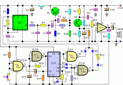
This circuit generates a two-tone effect very much alike the cuckoo song. It can be used for door-bells or other purposes thanks to a built-in audio amplifier and loudspeaker. Used as a sound effect generator it can be connected to external amplifiers, tape recorders etc. In this case, the built-in audio amplifier and loudspeaker may be omitted and the output taken across C8 and ground. There are two options: free running, when SW1 is left open, and one-shot, when SW1 is closed. In this case a two-tone cuckoo song will be generated at each P1 pressing.
Circuit diagram:
Circuit diagram:
Parts:
R1,R5___________1K 1/4W Resistors
R2_____________50K 1/2W Trimmer Cermet
R3______________8K2 1/4W Resistor
R4_____________82K 1/4W Resistor
R6______________1M 1/4W Resistor
R7,R17,R20,R21_22K 1/4W Resistors
R8,R10,R11,R19_10K 1/4W Resistors
R9____________150K 1/4W Resistor
R12_____________4K7 1/4W Resistor
R13___________100K 1/4W Resistor
R14___________220R 1/4W Resistor
R15,R22________20K 1/2W Trimmers Cermet
R16____________10R 1/4W Resistor
R18___________200K 1/2W Trimmer Cermet
C1,C11_________47nF 63V Polyester or Ceramic Capacitors
C2,C10,C12____220µF 25V Electrolytic Capacitors
C3____________220nF 63V Polyester or Ceramic Capacitor
C4_____________22nF 63V Polyester or Ceramic Capacitor
C5,C6,C8,C9___100nF 63V Polyester or Ceramic Capacitors
C7,C13,C14_____10µF 63V Electrolytic Capacitors
D1,D2,D3,D6__1N4148 75V 150mA Diodes
D4,D5_________BAT46 100V 150mA Schottky-barrier Diodes
Q1,Q2_________BC547 45V 100mA NPN Transistors
IC1____________7555 or TS555CN CMos Timer IC
IC2____________4093 Quad 2 input Schmitt NAND Gate IC
IC3____________4017 Decade counter with 10 decoded outputs IC
IC4___________LM386 Audio power amplifier IC
P1_____________SPST Pushbutton
SW1____________SPST Switch
SPKR___________8 Ohm Loudspeaker
Circuit Dis....
IC1 is wired as a square wave generator and produces both tones of the cuckoo song. The frequency of the higher one (667Hz) is set by means of Trimmer R2. When IC2D output goes low, a further Trimmer (R22) is added to IC1 timing components via D6, and the lower tone (545Hz) is generated. To imitate closely the cuckoo song, the square wave output of IC1 is converted to a quasi-sinusoidal wave form by R3, R4, C3 and C4, then mixed with the white noise generated by Q1, R6.
Q2 has two purposes: it mixes the two incoming signals and gates the resulting tone, shaping its attack and decay behavior by means of the parts wired around its Emitter. IC4 is the audio power amplifier driving the speaker and R15 is the volume control. The various sound and pause timings for the circuit are provided by the clock generator IC2A driving the decade counter IC3. Some output pins of this IC are gated by IC2C, IC2D and related components to drive appropriately the sound generator and the sound gate.
When SW1 is left open the circuit operates in the free-running mode and the cuckoo song is generated continuously. When SW1 is closed, the circuit generates two tones then stops, because a high state appears at the last output pin (#11) of the decade counter IC: therefore the count is inhibited by means of D1 feeding pin #13. The circuit is reset by a positive pulse at pin #15 of IC3 when P1 is pressed.
Setup:
Best results will be obtained if the two tones frequencies are set precisely, i.e. 667Hz for the first tone and 545Hz for the second: in musical terms this interval is called a Minor Third. Obviously a digital frequency counter, if available, would be the best tool to setup R2 and R22, but you can use a musical instrument, e.g. a piano or guitar, tuning-up the notes accurately by ear.
R1,R5___________1K 1/4W Resistors
R2_____________50K 1/2W Trimmer Cermet
R3______________8K2 1/4W Resistor
R4_____________82K 1/4W Resistor
R6______________1M 1/4W Resistor
R7,R17,R20,R21_22K 1/4W Resistors
R8,R10,R11,R19_10K 1/4W Resistors
R9____________150K 1/4W Resistor
R12_____________4K7 1/4W Resistor
R13___________100K 1/4W Resistor
R14___________220R 1/4W Resistor
R15,R22________20K 1/2W Trimmers Cermet
R16____________10R 1/4W Resistor
R18___________200K 1/2W Trimmer Cermet
C1,C11_________47nF 63V Polyester or Ceramic Capacitors
C2,C10,C12____220µF 25V Electrolytic Capacitors
C3____________220nF 63V Polyester or Ceramic Capacitor
C4_____________22nF 63V Polyester or Ceramic Capacitor
C5,C6,C8,C9___100nF 63V Polyester or Ceramic Capacitors
C7,C13,C14_____10µF 63V Electrolytic Capacitors
D1,D2,D3,D6__1N4148 75V 150mA Diodes
D4,D5_________BAT46 100V 150mA Schottky-barrier Diodes
Q1,Q2_________BC547 45V 100mA NPN Transistors
IC1____________7555 or TS555CN CMos Timer IC
IC2____________4093 Quad 2 input Schmitt NAND Gate IC
IC3____________4017 Decade counter with 10 decoded outputs IC
IC4___________LM386 Audio power amplifier IC
P1_____________SPST Pushbutton
SW1____________SPST Switch
SPKR___________8 Ohm Loudspeaker
Circuit Dis....
IC1 is wired as a square wave generator and produces both tones of the cuckoo song. The frequency of the higher one (667Hz) is set by means of Trimmer R2. When IC2D output goes low, a further Trimmer (R22) is added to IC1 timing components via D6, and the lower tone (545Hz) is generated. To imitate closely the cuckoo song, the square wave output of IC1 is converted to a quasi-sinusoidal wave form by R3, R4, C3 and C4, then mixed with the white noise generated by Q1, R6.
Q2 has two purposes: it mixes the two incoming signals and gates the resulting tone, shaping its attack and decay behavior by means of the parts wired around its Emitter. IC4 is the audio power amplifier driving the speaker and R15 is the volume control. The various sound and pause timings for the circuit are provided by the clock generator IC2A driving the decade counter IC3. Some output pins of this IC are gated by IC2C, IC2D and related components to drive appropriately the sound generator and the sound gate.
When SW1 is left open the circuit operates in the free-running mode and the cuckoo song is generated continuously. When SW1 is closed, the circuit generates two tones then stops, because a high state appears at the last output pin (#11) of the decade counter IC: therefore the count is inhibited by means of D1 feeding pin #13. The circuit is reset by a positive pulse at pin #15 of IC3 when P1 is pressed.
Setup:
Best results will be obtained if the two tones frequencies are set precisely, i.e. 667Hz for the first tone and 545Hz for the second: in musical terms this interval is called a Minor Third. Obviously a digital frequency counter, if available, would be the best tool to setup R2 and R22, but you can use a musical instrument, e.g. a piano or guitar, tuning-up the notes accurately by ear.
- Disconnect temporarily R22 from D6 anode.
- Connect the digital frequency counter to pin 3 of IC1.
- Adjust R2 in order to read 667Hz on the display.
- Connect R22 to negative ground and adjust it to read 545Hz on the display.
- Restore R22 - D6 connection.
Tuning by ear:
- Disconnect temporarily R22 from D6 anode.
- Disconnect C8 from Q2 Collector and connect it to R4, C4 and C5 junction.
- Adjust R2 in order that the tone generated by the loudspeaker is at the same pitch of the reference note generated by your musical instrument. This reference note will be the E written on the stave in the fourth space when using the treble clef.
- Connect R22 to negative ground and adjust it in order that the tone generated by the loudspeaker is at the same pitch of the reference note generated by your musical instrument. This second reference note will be the C-sharp written on the stave in the third space when using the treble clef.
- Restore R22 - D6 and C8 to Q2 Collector connections.
Notes:
- The master clock can be adjusted by means of R18.
- The percentage of hiss and sound in the mixing circuit, setting the tone character, can be varied changing R8 and R7 values respectively.
- Any kind of dc voltage supply in the 12 - 15V range can be used, but please note that supply voltages below 12V will prevent operation of the white noise generator.
- An amusing application of this circuit is to use a photo-resistor in place of P1, then placing the unit near the flashing lamps of your Christmas tree. A sweet cuckoo song will be heard each time the lamp chosen will illuminate.
Source: Red Free Circuit Models
Monday, October 20, 2014
Build a 4 Transistor FM Transmitter Circuit Diagram
4 Transistor FM Transmitter Circuit Diagram
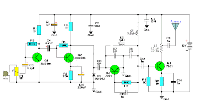
Build a 4 Transistor FM Transmitter Circuit Diagram. This 4 Transistor FM Transmitter Circuit Diagram provides an FM modulated signal with an output power of around 500mW. The input microphone pre-amp is built around a couple of 2N3904 transistors (Q1/Q2), and audio gain is limited by the 5k preset trim potentiometer.
The oscillator is a colpitt stage, frequency of oscillation governed by the tank circuit made from two 5pF ceramic capacitors and the L2 inductor. The output stage operates as a Class D amplifier, no direct bias is applied but the RF signal developed across the 3.9uH inductor is sufficient to drive this stage. The emitter resistor and 1k base resistor prevent instability and thermal runaway in this stage.
Build a 12V To 24V DC DC Converter Circuit Diagram
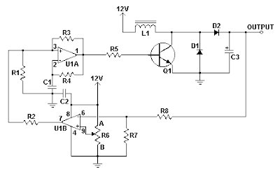
Build a 12V To 24V DC-DC Converter Circuit Diagram.This simple 12V To 24V DC-DC Converter Circuit Diagram can provide up to 24V from a 12V source. It can be used to run radios, small lights, relays, horns and other 24V accessories from a 12V vehicle with a maximum draw of about 800mA.
It can be used to charge one 12V battery from another, or step up the voltage just enough to provide necessary overhead for a 12V linear regulator. Using one op-amp as a square wave oscillator to ring an inductor and another op-amp in a feedback loop, it wont drift around under varying loads, providing a stable 24V source for many applications. With a wide adjustment in output this circuit has many uses.
12V To 24V DC-DC Converter Circuit Diagram
Parts
| R1, R2, R3, R4, R8, R7 | 6 | 100K 1/4W Resistor | |
| R5 | 1 | 470 Ohm 1/2W Resistor | |
| R6 | 1 | 10K Linear Pot | |
| C1 | 1 | 0.01uF Mylar Capacitor | |
| C2 | 1 | 0.1uF Ceramic Disc Capacitor | |
| C3 | 1 | 470uF 63V Electrolytic Capacitor | |
| D1 | 1 | 1N4004 Rectifier Diode | |
| D2 | 1 | BY229-400 Fast Recovery Diode | See Notes |
| Q1 | 1 | BC337 NPN Power Transistor | |
| U1 | 1 | LM358 Dual Op Amp IC | |
| L1 | 1 | See Notes | |
| MISC | 1 | Board, Wire, Socket For U1, Case, Knob For R6, Heatsink for Q1 |
Notes
- R6 sets the output voltage. This can be calculated by Vout = 12 x (R8/(R8+R7)) x (R6B/R6A).
- L1 is made by winding 60 turns of 0.63MM magnet wire on a toroidial core measuring 15MM (OD) by 8MM (ID) by 6MM (H).
- D2 can be any fast recovery diode rated at greater then 100V at 5A. It is very important that the diode be fast recovery and not a standard rectifier.
- Q1 will need a heatsink.
Sourced By Circuitsstream
Saturday, October 18, 2014
Build a Varying Brightness AC Lamp Circuit
Varying Brightness AC Lamp Circuit, an SCR is used to slowly vary the intensity of a 120 volt light bulb by controlling the time that the AC line voltage is applied to the lamp during each half cycle.
Varying Brightness AC Lamp Circuit Diagram

Caution:
The circuit is directly connected to the AC power line and should be placed inside an enclosure that will prevent direct contact with any of the components. To avoid electrical shock, do not touch any part of the circuit while it is connected to the AC power line. A 2K, 10 watt power resistor is used to drop the line voltage down to 9 volts DC. This resistor will dissipate about 7 watts and needs some ventilation.
Operation:
A couple NPN transistors are used to detect the beginning of each half cycle and trigger a delay timer which in turn triggers the SCR at the end of the delay time. The delay time is established by a current source which is controlled by a 4017 decade counter. The first count (pin 3) sets the current to a minimum which corresponds to about 7 milliseconds of delay, or most of the half cycle time so that the lamp is almost off. Full brightness is obtained on the sixth count (pin 1) which is not connected so that the current will be maximum and provide a minimum delay and trigger the SCR near the beginning of the cycle. The remaining 8 counts increment the brightness 4 steps up and 4 steps down between maximum and minimum. Each step up or down provides about twice or half the power, so that the intensity appears to change linearly. The brightness of each step can be adjusted with the 4 resistors (4.3K, 4.7K, 5.6K, 7.5K) connected to the counter outputs.
The circuit has been built by Don Warkentien (WODEW) who suggsted adding a small 47uF capacitor from ground to the junction of the current source transistor (PNP) to reduce the digital stepping effect so the lamp will brighten and fade in a smoother fashion. The value of this capacitor will depend on the 4017 counting rate, a faster rate would require a smaller capacitor.
Friday, October 17, 2014
Build a100W Inverter 12V to 220V Circuit Diagram
How to Build a100W Inverter 12V to 220V Circuit Diagram. When use the electric appliances that want 220V AC 50HZ, which have small-sized about 100Watt not exceed. By when you apply outside home, as a result have to have Mini power inverter about 100Watt, perform modify from work electricity forces of battery 12V give tall fair the work.
100W Inverter 12V to 220V Circuit Diagram

If you are New user electronics or want to economize or want to build electronics project use by oneself. I begs for to advise this circuit , because it uses , transistor number BC557 or the number replaces, perform oscillator generator. Then have power transistor 2N3055 numbers perform to drive coil transformer for converter voltage give tall go up 220V AC 50HZ at the electric power about 100 watt not exceed. When apply to transformer about 2A-3A. Picture circuit detail and like model PCB Board.
PCB

Sourced By www.circuitsstream.blogspot.com
Sunday, September 7, 2014
Build a Precision Increasing Buffer Wiring diagram Schematic
How to Build a Precision Increasing Buffer Circuit Diagram? This simple Precise Buffer Overflow Detection via Model Checking. increasing number of attacks that exploit such vulnerabilities. Precision Increasing Buffer Circuit Diagram adding an unity-gain buffer to your analog schema can increase its precision. For example, by itself, the op amp IC1 exhibits a maximum dVosldT of 1.8 /iV7°C and can drive a 600- load. Under these conditions, IC1 would dissipate 94 mW incrementally.
Precision Increasing Buffer Circuit Diagram
Thus, the op amp`s 0JA of 150°C/PFr would change its vqs by 25 juY. The buffer, IC2, will isolate IC1 from the load and eliminate the change in power dissipation in IC1, thereby achieving ICl`s minimum, rated offset-voltage drive. The loop gain of IC1 essentially eliminates the offset of the buffer. Almost any unity-gain buffer will work, provided that it exhibits a 3-dB bandwidth that is at least 5 times the gain-bandwidth product of the op amp.
Saturday, September 6, 2014
How to Build a 2 to 4 Wire Audio Converter
This audio converter schema maintains 40 dB of isolation between the two halves of entry and exit of a four-line son, while allowing a line connecting two son. A balancing potentiometer, R, adjusts the gain of zero lC2to crossing the inlet to the outlet .
The adjustment is done in terms of work just after installation by inserting a 1 kHz tone at the entrance of four son and setting R to the minimum output signal 82-ohm dummy-load resistor is placed between two wire terminals .
2 to 4 Wire Audio Converter Circuit Diagram
Saturday, August 30, 2014
Build a Wideband Antenna Preamplifier Wiring diagram Schematic
Build a Wide-band Antenna Preamplifier Circuit Diagram. This is a Wide-band Antenna Preamplifier Circuit Diagram. This schema has a gain of around 20 dB from 40 to 860 MHz, covering the entire VHF, FM, commercial, and UHF bands. A phantom power supply provides dc to the Preamplifier via the coaxial cable feeding the unit.
Wideband Antenna Preamplifier Circuit Diagram
Friday, August 29, 2014
Build a Inexpensive Isolation Transformer Wiring diagram Schematic
Build a Inexpensive Isolation Transformer Impromptus Setup Circuit Diagram. Using two 12-V filament or power transformers, an impromptu isolation transformer can be made for low-power (under 50 W) use in testing or servicing. SOI is an ordinary, duplex ac recept-able. Use heavy-wire connections between the 12-V windings because several amperes can flow.
Inexpensive Isolation Transformer Circuit Diagram
Sunday, August 24, 2014
Build a 300 Watt Subwoofer Power Amplifier Wiring diagram Schematic
The output devices are MJL4281A (NPN) and MJL4302A (PNP), and feature high bandwidth, excellent SOA (safe operating area), high linearity and high gain. Driver transistors are MJE15034 (NPN) and MJE15035 (PNP). All devices are rated at 350V, with the power transistors having a 230W dissipation and the drivers are 50W.
Having built a P68 using these transistors, I recommend them highly - the amplifier is most certainly at its very best with the high gain and linearity afforded by these devices. Note that there are a few minor changes to the schema (shown below).
High power amps are not too common as projects, since they are by their nature normally difficult to build, and are expensive. A small error during assembly means that you start again - this can get very costly. I recommend that you use the PCB for this amplifier, as it will save you much grief. This is not an amp for beginners working with Veroboard!
The amplifier can be assembled by a reasonably experienced hobbyist in about three hours. The metalwork will take somewhat longer, and this is especially true for the high continuous power variant. Even so, it is simple to build, compact, relatively inexpensive, and provides a level of performance that will satisfy most requirements.
Having built a P68 using these transistors, I recommend them highly - the amplifier is most certainly at its very best with the high gain and linearity afforded by these devices. Note that there are a few minor changes to the schema (shown below).
High power amps are not too common as projects, since they are by their nature normally difficult to build, and are expensive. A small error during assembly means that you start again - this can get very costly. I recommend that you use the PCB for this amplifier, as it will save you much grief. This is not an amp for beginners working with Veroboard!
The amplifier can be assembled by a reasonably experienced hobbyist in about three hours. The metalwork will take somewhat longer, and this is especially true for the high continuous power variant. Even so, it is simple to build, compact, relatively inexpensive, and provides a level of performance that will satisfy most requirements.
300W Sub woofer Power Amplifier Circuit Diagram
Fig 1
WARNINGS:- This amplifier is not trivial, despite its small size and apparent simplicity. The total DC is over 110V, and can kill you.
- The power dissipated is such that great care is needed with transistor mounting.
- The S300 is intended for intermittent duty on 4 Ohm loads, as will normally be found in a subwoofer. It is NOT intended for PA or any other continuous duty, and although it may work fine for may years, I absolutely do not recommend this.
- For continuous duty, do not use less than 8 Ohms.
- There is NO SHORT CIRCUIT PROTECTION. The amp is designed to be used within a subwoofer enclosure, so this has not been included. A short on the output will almost certainly destroy the amplifier.
DO NOT ATTEMPT THIS AMPLIFIER AS YOUR FIRST PROJECT
Please note that this amp is NOT designed for continuous high power into 4 Ohms. It is designed for intermittent duty, suitable for an equalized sub woofer system (for example using the ELF principle - see the Project Page for the info on this schema). Where continuous high power is required, another 4 output transistors are needed, wired in the same way as Q9, Q10, Q11 and Q12, and using 0.1 ohm emitter resistors.
Please note that this amp is NOT designed for continuous high power into 4 Ohms. It is designed for intermittent duty, suitable for an equalized sub woofer system (for example using the ELF principle - see the Project Page for the info on this schema). Where continuous high power is required, another 4 output transistors are needed, wired in the same way as Q9, Q10, Q11 and Q12, and using 0.1 ohm emitter resistors.
Continuous power into 8 ohms is typically over 150W, and it can be used in the form shown at full power into an 8 ohm load all day, every day. The additional transistors are only needed if you want to do the same thing into 4 ohms!
The schema is shown in Figure 1, and it is a reasonably conventional design. Connections are provided for the Internal SIM (published elsewhere on the Project Pages), and filtering is provided for RF protection (R1, C2). The input is via a 4.7uF bipolar cap, as this provides lots of capacitance in a small size. Because of the impedance, little or no degradation of sound will be apparent. A polyester cap may be used if you prefer - 1uF with the nominal 22k input impedance will give a -3dB frequency of 7.2Hz, which is quite low enough for any sub.
The input stage is a conventional long-tailed pair, and uses a current sink (Q1) in the emitter schema. I elected to use a current sink here to ensure that the amp would stabilise quickly upon application (and removal) of power, to eliminate the dreaded turn on "thump". The amp is actually at reasonably stable operating conditions with as little as +/-5 volts! Note also that there are connections for the SIM (Sound Impairment Monitor), which will indicate clipping better than any conventional clipping indicator schema. See the Project Pages for details on making a SIM schema.
The Class-A driver is again conventional, and uses a Miller stabilisation cap. This component should be either a 500V ceramic or a polystyrene device for best linearity. The collector load uses the bootstrap principle rather than an active current sink, as this is cheaper and very reliable (besides, I like the bootstrap principle :-)
It is in the output stage that the power capability of this amp is revealed. The main output is similar to many of my other designs, but with a higher value than normal for the "emitter" resistors (R16, R17). The voltage across these resistors is then used to provide base current for the main output devices, which operate in full Class-B. In some respects, this is a "poor-mans" version of the famous Quad "current dumping" schema, but without the refinements.
The Class-A driver is again conventional, and uses a Miller stabilisation cap. This component should be either a 500V ceramic or a polystyrene device for best linearity. The collector load uses the bootstrap principle rather than an active current sink, as this is cheaper and very reliable (besides, I like the bootstrap principle :-)
| All three driver transistors must be on a heatsink, and D2 and D3 should be in good thermal contact with the driver heatsink. Neglect to do this and the result will be thermal runaway, and the amp will fail. C11 does not exist on this schematic, so dont bother looking for it. It was "mislaid" when the schematic was prepared, and I didnt notice until someone asked me where and what it was supposed to be. Sorry about that. |
Although I have shown MJL4281A and MJL4302A output transistors, because they are new most constructors will find that these are not as easy to get as they should be. The alternatives are MJL21193/ MJL21194
Fig 2
Note: It is no longer possible to recommend any Toshiba transistors, since they are the most commonly counterfeited of all. The 2SA1302 and 2SC3281 are now obsolete - if you do find them, they are almost certainly fakes, since Toshiba has not made these devices since around 1999~2000.
Use a standard green LED. Do not use high brightness or other colors, as they may have a slightly different forward voltage, and this will change the current sinks operation - this may be a miniature type if desired. The resistors are all 1/4W (preferably metal film), except for R10, R11 and R22, which are 1W carbon film types. All low value resistors (1 ohm and 0.1 ohm) are 5W wire wound types.
Because this amp operates in "pure" Class-B (something of a contradiction of terms, I think), the high frequency distortion will be relatively high, and is unsuited to high power hi-fi. At the low frequency end of the spectrum, there is lots of negative feedback, and distortion is actually rather good, at about 0.04% up to 1kHz.
Power output into 4 ohms is over 250W continuous, and for transients exceeds 300W easily. Use of a big power transformer and massive filter caps will allow the amp to deliver close to 350W continuous, but if you really want to use it like that, I very strongly recommend the additional output transistors (see above comments on this topic).
Power Dissipation Considerations
I have made a lot of noise about not using this amp for continuous duty into 4 ohms without the extra transistors. A quick calculation reveals that at the worst case, the output and transistor voltage will be the same - i.e. at 28V. With 28V, load (and transistor) current is 7A, so the instantaneous dissipation is therefore 28 * 7 = 196W. This means that the four final transistors do most of the work, with the others having a relatively restful time.
Since I like to be conservative, I will assume that they contribute no more than about 1.5A (which is about right). This means that they only dissipate 48W, with the main O/P devices dissipating a peak of 74W each. The specified transistors are 130W, and the alternatives are 150W, so where is the problem?
The problem is simple - the rated dissipation for a transistor is with a case temperature of 25°C. As the amp is used, each internal transistor die gets hot, as does the transistor case - the standard derating curves must be applied. Add to this the reactive component as the loudspeaker drives current back into the amp, and it becomes all too easy to exceed the device dissipation limits.
Figure 1A shows the doubled output stage, with Q9, Q10, Q11 and Q12 simply repeated - along with the emitter resistors. Each 1/2 stage has its own zobel network and bypass caps as shown, as this is the arrangement if the dual PCB version is built. When you have this many power transistors, the amp will happily drive a 4 ohm load all day - with a big enough heatsink, and / or forced cooling (highly recommended, by the way).
A Few Specs and Measurements
The following figures are all relative to an output power of 225W into 4 ohms, or 30V RMS at 1kHz, unless otherwise stated. Noise and distortion figures are unweighted, and are measured at full bandwidth. Measurements were taken using a 300VA transformer, with 6,800uF filter caps. Mains voltage was about 4% low when I did the tests, so power output will normally be slightly higher than shown here if the mains are at the correct nominal voltage.
| Gain | 27dB |
| Power (Continuous) | 240W (4 ohms) |
| 153W (8 ohms) | |
| Peak Power - 5 ms | 185W (8 ohms) |
| Peak Power - 10 ms | 172W (8 ohms) |
| Input Voltage | 1.3V RMS |
| Noise | -63dBV (ref. 1V) |
| S/N Ratio | 92dB |
| Distortion | 0.4% |
| Distortion (@ 4W) | 0.04% (1 Khz) |
| Distortion (@ 4W) | 0.07% (10 kHz) |
| Slew Rate | > 3V/us |
| Power Bandwidth | 30 kHz |
Note that the "peak power" ratings represent the maximum power before the filter caps discharge and the supply voltage collapses. I measured these at 5 milliseconds and 10 milliseconds. Performance into 4 ohm loads will not be quite as good, as the caps will discharge faster. The supply voltage with zero power measured exactly 56V, and collapsed to 50.7V at full power into 8 ohms, and 47.5V at full power into 4 ohms.
Photo of Completed Prototype
As can be seen, this is the single board version. The driver transistors are in a row, so that a single sheet aluminium heatsink can be used for all three. Holes are provided on the board so the driver heatsink can be mounted firmly, to prevent the transistor leads breaking due to vibration. This is especially important if the amp is used for a powered subwoofer, but will probably not be needed for a chassis mounted system.
The driver and main heatsinks shown are adequate for up to 200W into 4 ohms with normal program material. The power transistors are all mounted underneath the board, and the mounting screw heads can be seen on the top of the board.
Deceptively simple, isnt it?
Power Supply
| WARNING: Mains wiring must be performed by a qualified electrician - Do not attempt the power supply unless suitably qualified. Faulty or incorrect mains wiring may result in death or serious injury. |
Figure 2 - Basic Power Supply Circuit
For 115V countries, the fuse should be 6A, and in all cases a slow blow fuse is required because of the inrush current of the transformer.
C1 must be rated for 240V AC (or 120V AC) operation - do not use standard 250V DC caps under any circumstance, as they will fail, and R1 will explode! This is not intended as humour - this is fact! C1 and R1 may be omitted in most cases, and if you cannot get a mains rated capacitor I suggest that you dont install these components.
C1 must be rated for 240V AC (or 120V AC) operation - do not use standard 250V DC caps under any circumstance, as they will fail, and R1 will explode! This is not intended as humour - this is fact! C1 and R1 may be omitted in most cases, and if you cannot get a mains rated capacitor I suggest that you dont install these components.
The supply voltage can be expected to be higher than that quoted at no load, and less at full load. This is entirely normal, and is due to the regulation of the transformer. In some cases, it will not be possible to obtain the rated power if the transformer is not adequately rated.
Bridge rectifiers should be 35A types, and filter capacitors must be rated at a minimum of 63V. Wiring needs to be heavy gauge, and the DC must be taken from the capacitors - not from the bridge rectifier.
Although shown with 4,700uF filter capacitors, larger ones may be used. Anything beyond 10,000uF is too expensive, and will not improve performance to any worthwhile degree. Probably the best is to use two 4,700uF caps per side (four in all). This will actually work better than a single 10,000uF device, and will be cheaper as well.
NOTE: It is essential that fuses are used for the power supply. While they will not stop the amp from failing (no fuse ever does), they will prevent catastrophic damage that would result from not protecting the schema from over-current conditions. Fuses can be mounted in fuseholders or can be inline types. The latter are preferred, as the supply leads can be kept as short as possible. Access from outside the chassis is not needed - if the fuses blow, the amplifier is almost certainly damaged.
Thursday, August 21, 2014
Build Intelligent Wire Loop Alarm Circuit With IC
Integrated schema anti-theft alarm system, wire or other lack of a simple schema. When the lack of wires or cords lacking. MOSFET, it is working or has input voltage at pin G and thus it has a high current flows through the pin D-S that Micro piezo siren was so loud.
Part List
R1 100K 1/2W 1% ResistorR2, R4 10K 1/2W 1% Resistor
R3 1 Meg 1/2W 1% Resistor
C1, C3 0.1uF Ceramic Disc Capacitor
C2 0.01uF Ceramic Disc Capacitor
IC1 4001UBE Quad 2-i/p NOR Gate
Q1 MPSA14 Low Power NPN Transistor
SIREN Micro piezo siren 12V DC 150mA, 110dB @ 1M
LOOP See “Notes”
The loop can be any type of hookup wire, with a maximum resistance of about 90K. Using very thin wire (40AWG, for example) will make a very sensitive trip wire, but will shorten the distance it can be strung due to the high resistance.
The siren can be replaced with a relay to drive external load
Wednesday, August 20, 2014
Build a 10000 Vdc Supply Wiring diagram Schematic
How to Build a 10000 Vdc Supply Circuit Diagram. A CMOS oscillator (U1A) drives. U1B through U1F, which drives Ql, which generates a 12-Vpp square wave across the primary of Tl. This square wave is applied to a rectifier-multiplier schema consisting of Dl through D10 (each is two 1N4007 diodes in series) and C3 through C12. About 10 kV is available.
10000 Vdc Supply Circuit Diagram
![10000]()
10000 Vdc Supply Circuit Diagram
Thursday, August 14, 2014
Build a Stabilized Capacitance Buffer Wiring diagram Schematic
This is a simplest Stabilized Capacitance Buffer Circuit Diagram. In this simple schema using Ql and Q2 constitute a simple, high-speed FET input buffer. Ql functions as a source follower, with the Q2 current source load setting the drain-source channel current. The LT1010 buffer provides output drive capability for cables or whatever load is required. Normally, this open-loop configuration would be quite drifty because there is no de feedback.
Stabilized Capacitance Buffer Circuit Diagram

The LTC1052 contributes this function to stabilize the schema. It does this by comparing the filtered schema output to a similarly filtered version of the input signal. The amplified difference between these signals is used to set Q2`s bias, and hence Ql `s channel current. Ql `s source line ensures that the gate never forward biases, and the 2000 pF capacitor at Al provides stable loop compensation.
The rc network in Al`s output prevents it from seeing high-speed edges coupled through Q2`s collector-base junction. A2`s output is also fed back to the shield around Ql`s gate lead, bootstrapping the schema`s effective in_put capacitance down to less than 1 pF.
Saturday, August 9, 2014
Build a Scanner Voice Squelch Wiring diagram Schematic
This Scanner Voice Squelch Circuit Diagram detects the presence of audio (voice) on the output of a scanner. If the scanner stops on a `dead carrier` or noise, the schema mutes the speaker to avoid annoying noise. Ul amplifies speech and drives rectifier D1/D2 and switch Ql. Comparator U3 drives speaker switch Ql and indicator LED1. Q2 completes the speaker path to ground. U2 is an audio amplifier to drive the speaker. R3 is a volume control. PL1 connects to the scanner speaker or to the headphone jack .
Build a Scanner Voice Squelch Circuit Diagram

Subscribe to:
Posts (Atom)
