Showing posts with label driver. Show all posts
Showing posts with label driver. Show all posts
Monday, November 17, 2014
Power supply with driver TEA1507
Power supply with driver TEA1507 is mostly used by TV branded PHILIPS. Power Supply has an efficiency rate of up to 90% - thus requiring less cooling, as well as stand-by power required is less than 1 watt.
Power Supply with TEA driver is equipped with a variety of surge protector that has a high reliability - not easily damaged if any part of a damaged power supply circuit and power transistor or FET heat is not easily damaged. Power supply circuits are dapatapat working on ac input voltage between 85 up to 275v. The way it works with the driver circuit power supply TEA 1507 is quite simple, so easy tracking of damage to the circuit.
The picture above is the basic power supply circuit with TEA1507

Monday, November 3, 2014
SSL3250A PHOTO FLASH LED DRIVER ELECTRONIC DIAGRAM

SSL3250A PHOTO FLASH LED DRIVER ELECTRONIC DIAGRAM
These properties caused this device has long battery life and low power strain. Another features that this device has are protecting the battery and LED from overloading, trouble free operation such as overtemperature, over voltage, time-out function, undervoltage lockout, and feedback shorted protection.
Wednesday, October 22, 2014
Motor driver L298 Circuit
DC motor driver with H-Bridge IC L293D
IC H Bridge DC motor driver L298 has two H-Bridge circuit in it, so it can be used to download the drive two DC motors. H Bridge DC motor driver L298 each can deliver currents up to 2A. However, in use, the H Bridge DC motor driver L298 can be used in parallel, so the ability to deliver the H Bridge DC motor driver L298 flow into 4A. The consequences of the installation of H Bridge L298 DC motor driver with the parallel mode, you need 2 pieces Bridge H L298 DC motor driver to control two DC motors using H bridge DC motor driver L298 in parallel mode.
H Bridge Pin IC L298 DC motor driver which is connected in parallel operation mode:* OUT1 connected to OUT4.
* OUT2 OUT3 linked.
* IN1 is connected to IN4.
* IN2 connected to IN3.
* ENABLE ENABLE A linked to B.

OUT1/OUT4 and OUT2/OUT3 associated with DC motors to be controlled.
Please note that the output of the L298 does not have a safety diode. Thus, the need to add two diodes - flyback diodes, with appropriate current capability, at any point output.
Thursday, September 18, 2014
Simple 4A High Speed Low Side Gate Driver
The UCC27518 and UCC27519 single-channel, high-speed, low-side gate driver device is capable of effectively driving MOSFET and IGBT power switches. Using a design that inherently minimizes shoot-through current, UCC27518 and UCC27519 are capable of sourcing and sinking high, peak-current pulses into capacitive loads offering rail-to-rail drive capability and extremely small propagation delay typically 17 ns.
The UCC27518 and UCC27519 provide 4-A source, 4-A sink (symmetrical drive) peak-drive current capability at VDD = 12 V. The UCC27518 and UCC27519 are designed to operate over a wide VDD range of 4.5 V to 18 V and wide temperature range of -40°C to 140°C. Internal Under Voltage Lockout (UVLO) circuitry on VDD pin holds output low outside VDD operating range.
The UCC27518 and UCC27519 provide 4-A source, 4-A sink (symmetrical drive) peak-drive current capability at VDD = 12 V. The UCC27518 and UCC27519 are designed to operate over a wide VDD range of 4.5 V to 18 V and wide temperature range of -40°C to 140°C. Internal Under Voltage Lockout (UVLO) circuitry on VDD pin holds output low outside VDD operating range.
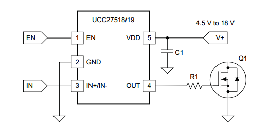
Features
- Low-Cost, Gate-Driver Device Offering Superior Replacement of NPN and PNP Discrete Solutions
- Pin-to-Pin Compatible With TI’s TPS2828 and the TPS2829
- 4-A Peak Source and 4-A Peak Sink Symmetrical Drive
- Fast Propagation Delays (17-ns typical)
- Fast Rise and Fall Times (8-ns and 7-ns typical)
- 4.5-V to 18-V Single Supply Range
- Outputs Held Low During VDD UVLO (ensures glitch free operation at power-up and power-down)
- CMOS Input Logic Threshold (function of supply voltage with hysteresis)
- Hysteretic Logic Thresholds for High Noise Immunity
- EN Pin for Enable Function (allowed to be no connect)
- Output Held Low when Input Pins are Floating
- Input Pin Absolute Maximum Voltage Levels Not Restricted by VDD Pin Bias Supply Voltage
- Operating Temperature Range of -40°C to 140°C
- 5-Pin DBV Package (SOT-23)
Device Uses
- Switch-Mode Power Supplies
- DC-to-DC Converters
- Companion Gate Driver Devices for Digital Power Controllers
- Solar Power, Motor Control, UPS
- Gate Driver for Emerging Wide Band-Gap Power Devices (such as GaN)
Sunday, August 31, 2014
Full Rail Excursions Line driver Wiring diagram Schematic
Full Rail Excursions Line driver Circuit Diagram. This is a Line driver provides full rail excursions schema diagram. The logic input is applied to opt-isolators Ul and U2 with, respectively, npn and pnp emitter follower outputs. Dc balance is adjusted by potentiometer R2. The emitter followers drive the gates of Ql and Q2, the complementary TMOS pairs.
With a ±12 V supply, the swing at the common source output point is about 12 V peak-to-peak. By adding a ± 18-V boost schema, as shown, the output swing can approach the rail swing. This schema applies the output to transformer Tl, which is rectified by diode bridge D3, regulated by U3 and U4, and then applied to the collectors of Ul and U2. Diodes Dl and D2 are forward-biased when 12-V supplies are used, but they are back-biased when the 18-V boost is used.
Full Rail Excursions - Line driver Circuit Diagram

Subscribe to:
Posts (Atom)
