Showing posts with label switch. Show all posts

Friday, November 14, 2014

VOLTAGE COMPARATOR SWITCH

This circuit will provide an indication whenever the input voltage differs from two defined limits, V1 and V2. The limits are adjustable and the circuit made to trigger from the adjustable "window". The supply voltage, Vcc must be higher than the highest input voltage by at least 2 volts. One application here is to monitor a 12V car battery. V1 could be set to 14V and V2 to 11V thus giving an indication of over charge or a weak battery.

Circuit Diagram


Fig. 1

Important Points

Only pins 7 and 4 (power supply), pin 6 (output) and pins 2 and 3 (inverting and non-inverting inputs) are used. All other pins are not connected. The pinout for the CA3140 is shown below.

Fig. 2

The op-amps used here are MOSFET CA3140. They are used to advantage as they have very little output offset voltage and can switch down to near 0 volts. If any other op-amp is used such as LF351 or CA741 then it will be necessary to have an offset null control. This is just a 10k preset contacted between pins 1 and 5, the wiper connected to the negative supply rail or op-amp pin 4. With this circuit either op-amp will light the LED if the input voltage goes out of limits, the two 1N4148 diodes forming an "AND"-gate at the output. The input voltage to be monitored is fed via a series 10k resistor to inputs of both op-amps. If the input voltage is greater than the limit set by V1 then the CA3140 will swing its output to almost the full supply voltage and light the LED. Similarly, if the input voltage is less than the limit defined by V2 then this op-amp will swing towards Vcc and light the LED.
Read More..

Thursday, October 23, 2014

Double Pole Switch Installation

In order to control electrical loads such as heating in the picture below using double pole switch. Double pole switch consists of four terminals. And electric heating load consists of three terminals. In the second switch terminal to get into each phase line (L) and the neutral line (N). While the other two terminals each connected to two terminal heating load. One other terminal on the body burden, directly connected to the grounding line.
Electrical
 a. Electrical circuit drawings double pole switch

Double
b. Double pole switch wiring drawings

Image
c. Image channel double pole switch
Read More..

Wednesday, October 22, 2014

12V Touch Switch Exciter

This circuit is designed to generate a 20KHz pseudo sine wave signal that can power about 50 remote touch activated switch circuits.  It can support a cable length of about 2500 feet.  A typical remote switch circuit is also shown as well as a receiver circuit for those switches.


Source: DiscoverCircuits
Read More..

Thursday, October 2, 2014

Simple IC 555 Touch Activated Switch Circuit

  1. An LED with a suitable series resistance may be included in the circuit and placed in the centre of the touch plate to indicate when the relay is activated. In cases of severe stray pick-up, the unit should be enclosed in a metal casing that should be grounded.
  2. In the circuit, some special precautions have been taken to avoid interference pick-up, to which TTL ICs are especially prone.
  3. To minimise stray pick-up, the interconnections should be as short as possible.
  4. Capacitor C2 is rather large compared to the conventional value (0.0lp.F) used in this position. This modification has proved quite effective.
  5. The power supply shown provides an appropriate DC voltage to drive a conventional relay.
  6. The value of Rl is best chosen by trail and error, and is a compromise between sensitivity and immunity from stray pick-up, Its value lies in the range l.8M to IOM. Rl may be excluded altogether.
  7. If the unitis situated away from the touch sensor, a shielded wire should be used for the connection.
  8. Tl acts as an inverter and converts a rising edge into a falling edge. Transistor T2 is used to provide sufficient drive capability to drive the relay. The external load is connected across the g relay contacts.
  9. An additional decoupling capacitor ((0.0lp.F) may be added as close as possible to the supply terminals of IC 7493. The prototype was constructed on a conventional bread- board.
  10. The circuit basically comprises a touch activated mono- stable vibrator using an NE555 IC, which activates the ITL s 7493 IC used as a bistable. , .
  11. Another modification is the addition of Cl-Rl parallel combination.
  12. The monostable is touch activated and it provides the triggering input to the bistable. However, the bistable triggers only on the falling edge of the monostable output pulse.
  13. This causes a time delay before the load is actually activated. To avoid this, Tl is introduced. 
Read More..

Saturday, September 20, 2014

TL594 12V DC Switch Mode Power Supply Wiring diagram Schematic

In recent years, the use of switch mode power supply (SMPS) has become more comon as more applications demand for greater power eficiency. It makes use of semiconductor (mostly MOSFET) fast switches to switch DC input that has been rectified at high frequency. The advantages of high frequency switching are that it reduces the size of inductor, capacitors & transformer used. Other advantages of switching power supply over linear power supply are :

1) High Efficiency (up to 90% and above for nice design).
2) Output can be higher than input.
3) Able to operate over a variety of input power supply.
4) Able to have over output.

The setback of using SMPS compared to linear power supply is that it generates electrical noise which contributes to electromagnetic compatibility design issues & more part count.

Buck Converter SMPS
The SMPS schema below from Power Integration makes use of LNK304 as its high frequency switch. Take note that this schema is non isolated type which means that the output is not electrically isolated from the input & all testing ought to be completed using an isolation transformer to provide the AC line input to the board.

Make positive that you have electrical safety knowledge & experience before you embark on doing this project.

12V DC Switch Mode Power Supply Circuit Diagram

12V


Read More..

Thursday, September 18, 2014

12v Light Dark Switch

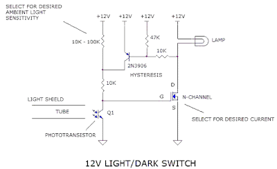
Often, for certain low voltage lighting systems; you would like to turn off the lights during the bright light of the day.  Most commercial day/night switches are designed for AC lighting.  This hobby circuit below was designed for a 12v DC system.  But, it could be modified for other voltage as well.  It uses an inexpensive photo-transistor as the light detector.  An n-channel FET is used to switch power to the lights.  A transistor circuit is included to provide some hysteresis.  

This keeps the circuit from fluttering the light during the transition from day to night and night to day.  It is recommended that a plastic tube be placed over the transistor to prevent it from being illuminated by the lights it is controlling.  By selecting the appropriate power FET, the circuit could control over 100 watts worth of 12v lighting.   (July 22, 2008)


Circuit Project:12v LightDark Switch
 
 
Source: DiscoverCircuits
Read More..

A Headphone Monitoring Switch

In any recording situation, monitoring is critical to make sure youre getting what you want on tape. This is just as true in field recording, but in most cases, ones monitoring options are severely limited--stereo headphone is the only choice.

Headphone Monitoring Switch  :

A headphone monitoring Switch-Circuit Daigram

Since I often use dual-mono mics, hearing a stereo feed of the two is not always convenient. I wanted the option to hear JUST the left mic in BOTH ears, or just the right mic in both ears, as well as a normal stereo signal. This is simple enough to do with a big rotary switch. When completed, you can create a little box that your headphones plug into, which in turn is plugged into the stereo phone output of your deck. Then, by turning the knob on the switch box, you can hear normal stereo, left-only mono, right-only mono, left+right mono and even left-right reversed stereo (or normal stereo again). 

Note the use of summing resistors in the left+right mono section. This was an attempt to prevent the two outputs from "fighting" each other if there were very different voltages in left and right outputs. I used 8 ohm resistors here, but a higher value might be better. Maybe ~20 ohms? Also, I initially decided to put normal stereo on both ends of the switchs travel so Id always be able to find it without looking. However, I sometimes wish to have left-right reversed. If youd like to try this, simply swap the leads on one of the "normal stereo" connections. 

One final caveat: The left only/right-only mono positions are -6dB down, since only one half of the decks headphone amp is driving your phones when the switch is in those positions. 


Source by : Ecircuitslab
Read More..

Monday, September 8, 2014

2 Way Remote Ac Switch Hookup Wiring diagram Schematic

Once it is connected to your network, the remote access via the App is a nice feature.. This switching arrangement is the type of arrangement used in both domestic and industrial environments to allow a light or other ac-operated device to be controlled from more than one location.

2 Way Remote Ac Switch Hookup Circuit Diagram

2

Read More..

Monday, September 1, 2014

Using 555 Timer Voltage Controlled Switch

In this schema the 555 timer is used in a novel way, as a voltage controlled switch.The old and omnipresent NE555 can be very good at something it was not meant for: driving relays or other loads up to 200 mA. The picture shows an example schema: if the input level rises over 2/3 of the supply voltage - it will turn on the relay, and the relay will stay on until the level at the input drops below one third of the supply voltage.

If the relay and D1 were connected between pin 3 and ground, the relay would be activated when the input voltage drops below one third, and deactivated when the input voltage goes over two thirds of the supply voltage. It is also a nice advantage that the input requires only about 1 uA, which is something bipolar transistors cant compete with. (This high impedance input must not be left open.) A large hysteresis makes the schema immune to noise. The output (pin 3) can only be either high or low (voltage-wise), and it changes its state almost instantenously, regardless of the input signal shape.

Voltage Controlled Switch Circuit Diagram


Voltage

The voltage drop across the NE555s output stage (at 35-100 mA) is 0.3-2.0 V, depending on the way the relay is connected and the exact current it draws. D1 is absolutely vital to the safety of the integrated schema.
Read More..

Thursday, August 28, 2014

Simple Dc Static Switch Wiring diagram Schematic

This is a Simple Dc Static Switch Circuit Diagram. This schema is a static SCR switch for use in a dc schema. When a low power signal is applied to the gate of SCR1, this SCR is triggered and voltage is applied to the load. The right hand plate of C charges positively with respect to the left hand plate through Rl. 

 Simple Dc Static Switch Circuit Diagram

 simple dc static switch circuit diagram


When SCR2 is triggered on, capacitor C is connected across SCR1, so that this SCR is momentarily reverse biased between anode and cathode. This reverse voltage turns SCR1 off provided the gate signal is not applied simultaneously to both gates. The current through the load will decrease to zero in an exponential fashion as C becomes charged.


Read More..

Saturday, August 16, 2014

Electronic Push on Push off Switch Wiring diagram Schematic

This is a simple Electronic Push-on Push-off Switch Circuit Diagram. Transistors Ql and Q2 make up the flip-flop while Q3 drives a reed relay. When power is first applied to the schema, Ql and Q3 are conducting and Q2 is cut off. Momentarily closing SI causes the flip-flop to switch states—Ql cuts off and Q2 conducts. When Q2 is conducting, its collector drops to around 0.6 volt. 

 Electronic Push-on Push-off Switch Circuit Diagram


Electronic


That prevents base current from flowing into Q3 so it is cut off, de-energizing relay Kl. The flip-flop changes state every time SI is pressed. Capacitors Cl and C2 ensure that Ql is always the transistor that turns on when power is first applied to the schema. When power is first applied to the basic flip-flop, the initial status is random—Ql and Q2 both try to conduct and, usually, the transistor with the higher gain will take control, reaching full conduction and cutting off the other one. 

However, differences in the values of the collector and coupling resistors will also influence the initial state at power-on. With C2 in the schema, it and R4 form an R-C network that slightly delays the rise in Q2s base voltage. That gives Ql sufficient time to reach saturation and thus take control.
Read More..